Download
1 / 18
200 likes | 508 Views
Design and execution of a comprehensive PCB Management Plan for Kazakhstan. IPEN Global Assembly 19 October 2010. General information. Implementing agency: UNDP-Kazakhstan Project duration: 5 years Project implementation modality – NEX - Ministry of Environmental Protection -

E N D
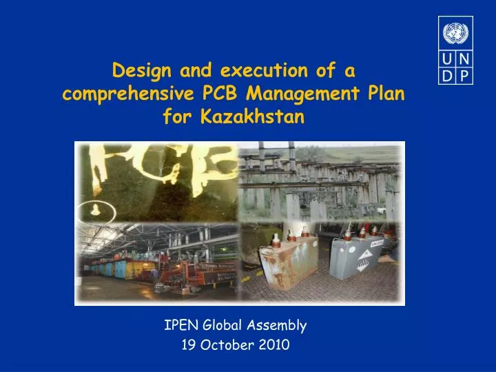
Design and execution of a comprehensive PCB Management Plan for Kazakhstan IPEN Global Assembly 19 October2010
General information • Implementing agency: UNDP-Kazakhstan • Project duration: 5 years • Project implementation modality – NEX - Ministry of Environmental Protection - • Office location: Astana • GEF grant: USD 3,300,000
Project Management Steering Committee Beneficiary Ministry of Environmental Protection Chairman National Director UNDP Quality Assurance UNDP GEF National coordinator (MoEP) National project manager Project team Project Assistant Experts Consultants
Project financing • Financial contribution : • In-kind contribution : US$ 10,901,356 - Government of Kazakhstan • Total project budget: US$ 20,834,680
Project Objective: Ensure minimization of PCB releases and subsequent health and environmental impacts through systematic capacity development for sound PCB management in the country
Facts and figures • Production of PCB capacitors until 1989 • 4 PCB hotspots • Ust-Kamenogorsk storage pond • Ust-Kamenogorsk capacitor plant • Ekibastuz power sub-station • Dariyal-U former military base • 116 pure PCB transformers (~ 950 tons) • 56 000 PCB capacitors (~ 2,500 tons) • 225,000 tons of highly PCB contaminated soil
PCB equipment map of Kazakhstan PCBcapacitors PCB capacitor batteries PCB transformers
Project Outcomes Outcome 1 - Regulatory and administrative strengthening for sound PCB management Outcome 2 - Capacity building for sound PCB management, identification of additional PCB sources Outcome 3 - Disconnecting, dismantling and disposal of 850 tons of PCB transformers (in partnership with ArcelorMittal Temirtau) Outcome 4: Regionally organized secure storages and disposal of PCB capacitors
Regulatory and administrative strengthening for sound PCB management • Output 1.1: Environmental Code and other PCB related legislation reviewed, changes developed. Environmental Code revised to include a chapter on PCB management and disposal. • Output 1.2: Responsibilities vis-a-vis International Chemicals´ Conventions in the government re-aligned • Output 1.3: Detailed PCB rules, guidelines, incentive schemes developed • Output 1.4: Capacity for implementing and knowledge of PCB regulations and guidance among public sector actors, including training of customs department in PCB identification, enhanced. • Output 1.5: Awareness raising campaigns on PCB risks and regulatory requirements among authorities and wider public conducted.
National PCB Management Plan Framework “PCB Manual” “PCB Action Plan” National Chemical Safety Policy A. PCB Management Guidelines • C. Action Plan 2011-2015 • Objectives & Targets • Components/Outcomes (e.g. Inventory Plan) • Stakeholders/Partners • KPIs/deliverables • D. Budget Program 2011-2015 • National level (Government) • Regional level (local authorities) • Local level (PCB holders) • B. PCB Regulations • Rules of PCB inventory (2010) • Stocktaking and monitoring rules (2011) • Rules of PCB equipment phase-out (2011) • Technical requirements for temporary PCB/HW storage facilities (2011) • Rules of packaging, labeling and transportation of PCB (2011) • Technical requirements for incineration of hazardous waste (2011-2012) • Others (?) – 2012-2015 E. Monitoring and Evaluation Plan 2011-2015
Other key elements of PCB Management Plan • Stakeholder Engagement Strategy • Communication Strategy • PCB Information Management Systems: • Web site • Databases • GIS-based Information Management System. 2010 – 2011: design and development phase • 2010 – design (regulation) • 2011 – planning (management system) • + inventory (initial phase)
Capacity building for sound PCB management, identification of additional PCB sources • Output 2.1: Improved capacities of PCB holders for sound PCB management • Output 2.2: PCB holder-wise management and replacement plans • Output 2.3: PCB inventory expanded and updated • Output 2.4: Enhanced PCB analysis preparedness at State Hydro-meteorological services and Ministry of Health laboratories • Output 2.5: Risk based priority setting tools for PCBs management initiatives developed..
Key indicators • National Inventory Plan 2011-2015 • Setting clear targets for closed and open systems • Setting deadlines for large companies, small and medium size companies, municipalities • PCB Management Plans for 20 companies - first 3 years • Accreditation of reference POPs laboratory • Training and awareness raising plan 2011-2015 (PCB MP)
Replacement, setting-up safe dismantling of 850 tons of PCB transformers and their safe disposal • Output 3.1: Phase-out and procurement of replacement transformers planned and scheduled • Output 3.2: Transformers disconnected, drained, dismantled and cleaned, metals recycled • Output 3.3: Disposal of oils and associated waste
Regionally organized secure storages and disposal of PCB capacitors • Output 4.1: Secure, temporary PCB storage facilities identified, constructed/upgraded • Output 4.2: Safe operation of storage sites secured • Output 4.3: PCB collection and disposal put in place and implemented • Output 4.4: 15,000 PCB capacitors at Darial-U capacitor site disconnected, packed and stored. • Output 4.5: Clean-up premises and pack all potentially PCB contaminated wastes. • Output 4.6: Transportation and disposal of approximately 600 tons of PCBs and associated waste disposed.
Working area Freely accessible area 10 m 21, 32 m Temporary storage Scale Driveway 8, 2 m2 Transformer draining area Input area Output area 5,1 m2 10,1 m2 2 x 20 m3 12,1 m2 Crane Crane PCB oil tank Capacitor draining area 14,4 m 6,2 m2 Material sluice Personnel sluice Transformer draining area 10,2 m2 Storage for materials / tools 16,1 m2 5, 2 m2 Air outlet 3,1 m2 Forklift Emergency exit Entrance Key indicators • Disposal of Dariayl-U 6,000 capacitors (~200 t) • Establishment of 3 storage facilities for PCB waste (capacitors, transformers) • 200 tof additional PCB waste collected and disposed • Design of transportation scheme (inside Kazakhstan, transportation routes to EU region and from Central Asian countries) – PCB MP • Dariyal-U clean-up project developed