Download
1 / 4
40 likes | 48 Views
Verifying the integrated circuit designs and restricting the violations made through the builders are the initial steps for chip manufacturing. The rising needs for the multiple points in electronic units require superior chip designs with excessive computational abilities.

E N D
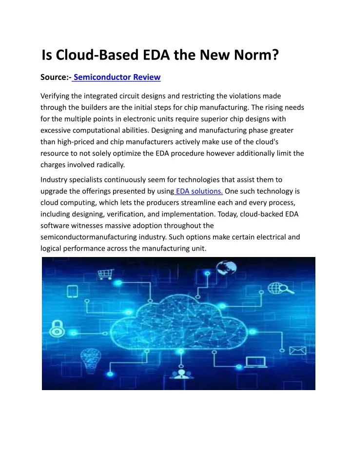
Is Cloud-Based EDA the New Norm? Source:-Semiconductor Review Verifying the integrated circuit designs and restricting the violations made through the builders are the initial steps for chip manufacturing. The rising needs for the multiple points in electronic units require superior chip designs with excessive computational abilities. Designing and manufacturing phase greater than high-priced and chip manufacturers actively make use of the cloud's resource to not solely optimize the EDA procedure however additionally limit the charges involved radically. Industry specialists continuously seem for technologies that assist them to upgrade the offerings presented by usingEDA solutions. One such technology is cloud computing, which lets the producers streamline each and every process, including designing, verification, and implementation. Today, cloud-backed EDA software witnesses massive adoption throughout the semiconductormanufacturing industry. Such options make certain electrical and logical performance across the manufacturing unit.
Cloud science integrated into EDA solutions enables the chip producers to accurately affirm the designs of the circuit, and locate and restore violations made through the builders as a step before layout execution. Such superior points in EDA equipment minimize the large amount of manufacturing cost and time. This additionally eliminates the chances of manufacturing errors. Cloud-influenced EDA options centralize both block-level designs and permitted sign-off designs of the circuit at semiconductor fabrication plants. Circuit diagram checking softwareprogram provides high-performing secure, and scalable solutions for physical circuit verification. Cloud technology's capacity to create a seamless verbal exchange platform lets the dressmaker teams speak with the extraordinary operation teams in real-time and make indispensable enhancements in accordance to the up-graded regulations, and even customize according to the digital system requirement. Cloud-based options enable electronic engineers to make bigger protection measures for checking out circuit format digitally throughout fabrication. The increasing needs fortrendy electronicdeviceswith excessive computation and seamless performance competencies motivate semiconductor producers to adopt such incredible solutions for format verification and evaluation processes. How eFPGA Future-Proofs Data Centers With the technology at a crossroads, data centers have become the sweet spot of the technology vendors, showing strong revenue growth and attracting new system solutions inboth hardware and software wings. The dynamism of growing markets has forced data center designers to move away from customized hardware architectures towards commoditized hardware with high port counts, high performance, and low power consumption. This approach supports scalability and redundancy while minimizing cost and the need to expand or renovate the installed plant and its associated infrastructure. As a result, data
centers are looking at ways to future proof their infrastructure, and there enters FPGA. Data centers use thousands of chips, including arm processors, networking processors, andnetwork interface chips (NICs). These chips are expensive to make, and these costs are shared with the data centers over time. What's been needed here is FPGA that is flexible, scalable, low cost, and high-performing. Here comes embedded FPGA (eFPGA), which is entrenched directly onto chips and is reconfigurable. This allows eFPGA to provide higher performance at lower power. eFPGA also delivers noteworthy performance benefits, especially with regards to the bandwidth the FPGAs can have with the rest of the chips. Even a small eFPGA can have 1,000 inputs and 1,000 outputs with data rates greater than 500MHz in 28nm or more in 16/14nm. eFPGA can provide parallel processing that significantly improves performance over the serial processing of MPUs. Its reconfigurability allows eFPGA to accelerate more than one task as workloads require. This added performance is critical in data centers. The ability to accelerate critical code is something that chip designers should be evaluating today, and this is whatdata center operatorsshould be asking for in their chips. Being more programmable and reconfigurable helps data centers to keep up with the constantly changing standards and protocols. Previously, data centers had to
wait for new hardware and chips to meet these new requirements. This is all changing with eFPGA, and data centers will soon be able to quickly and seamlessly stay meet the rising bandwidth demands. Twitter|Semiconductor Review LinkedIn|Semiconductor Review