Download
1 / 48
480 likes | 764 Views
Manufacturing. A Modern CMOS Process. Dual-Well Trench-Isolated CMOS ... Brewer, adapted from MOSIS Data, Digital Integrated Circuits2nd. Manufacturing. 80 nm Lines ...

E N D
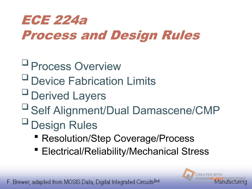
1. ECE 224a Process and Design Rules Process Overview
Device Fabrication Limits
Derived Layers
Self Alignment/Dual Damascene/CMP
Design Rules
Resolution/Step Coverage/Process
Electrical/Reliability/Mechanical Stress
2. A Modern CMOS Process
3. Circuit Under Design
4. Its Layout View
5. The Manufacturing Process Photo-Lithography
Mask to Resist
Resist to Pattern Layer
Process (Implant/Etch/Oxide/Nitride/�)
Cleanup (Clean/Planarization/Anneal)
Setup next Layer for Processing
6. Photo-Lithographic Process
7. Patterning of SiO2
8. CMOS Process Walk-Through
9. CMOS Process Walk-Through
10. CMOS Process Walk-Through
11. CMOS Process Walk-Through
12. Advanced Process Modules
13. Lithography for 0.1um Node
14. Poly Gate Etch ? 100nm
15. 12A Gate Oxide
16. Advanced Metallization
17. Interconnect RC Trend
18. Design Rules What can be fabricated?
Resolution Limits
Light Source (357nm, 254nm, 193nm, ?)
Contact/Phase Masking
Surface State (Reflection/Scattering)
Material Limits
Step Coverage
Porosity/Defect Propagation
Mechanical/Thermal Stress
19. Design Rules II Electrical Limits
Electrical Fields (MV/cm)!
Parasitic Conductivity/Devices (Latchup/ESD)
Joule Heating (Electro-Migration)
Defect Probability
Contact/Via Replication
Grid-Based Power/Ground Networks
Advance Lithography
Rule Explosion/Failure of Locality
CMP Area Rules/Antenna Rules
20. 85nm Poly Gate Profile
21. CL013 Core Device
22. 0.13/0.18 Comparison
23. 3D Perspective
24. Poly-SiGe Gate
25. Design Rules III Interface twixt designer and process engineer
Unit dimension: Minimum Feature Size
scalable design rules: lambda
absolute dimensions: (Vendor rules)
Process Design Layers
Derived Layers
26. CMOS Process Design Layers
27. Intra-Layer Design Rules
28. Transistor Layout 3.1 FET length 2 (min)
3.2 FET spacing 3
3.3 Poly Overlap 2
3.4 Active Overlap 3
3.5 Space 1
29. Active Contact I 6.1 Size 2x2
6.2 Enclosure 1.5
6.3 Spacing 3
6.4 Space to FET 2
30. Poly Contact I 5.1 Size 2x2
5.2 Enclosure 1.5
5.3 Spacing 3
5.4 Space to FET 2
31. Via (m1 to m2) 8.1 Size 2x2
8.2 Spacing 3
8.3 Enclosure 1
8.4 Space to Contact 2
8.5 Space to Poly/Act 2
32. Select Layer
33. Layout Editor
34. Design Rule Checker
35. Sticks Diagram
36. Layout Guidelines I Group Transistors into Cells
Plan inter-cell wires first (Sticks)
Oversize Power Grids (Cell Default >6)
Frequent Substrate Contacts/Well Plugs
Every Well (even one will kill design!)
Max distance to plug/contact 5-8 microns
Set a large user grid e.g. 1-2 lambda
Don�t optimize until you know the constraints
Plan for Change and Optimization
37. Layout Guidelines II Current Limits
1 mA/mm2 Avg. current limit (50C)
Strongly Temp Dependent (Al)
Failures typically occur at vias and contacts
Vias often Tungsten (higher resistance)
Wide Wires need via arrays!
Transistor Contacts
Active is highly resistive
Avoid High Density Currents
38. Packaging
39. Packaging Requirements Electrical: Low parasitics
Mechanical: Reliable and robust
Thermal: Efficient heat removal
Economical: Cheap
40. Bonding Techniques
41. Tape-Automated Bonding (TAB)
42. Flip-Chip Bonding
43. Cu Flip-Chip Technology
44. Package-to-Board Interconnect
45. Package Types
46. Package Parameters
47. Multi-Chip Modules
48. Lecture Problems 2 Why is there a spacing rule between via�s and contacts and/or vias and other vias? How is it eliminated in deeper (smaller) processes?
Draw a schematic and stick layout for a 3-input 2-output adder cell (output is sum and carry). Design as two cells: a cell producing ~Cout and another cell producing Sout(a,b,c,~Cout). Design Sue schematics and Max Layout for the two cells with minimum size transistors and turn in check plots.
Guard Rings consist of n and p contact regions with continuous metal connections. They are often used to surround and isolate sensitive devices. How do they work?
Very wide metal (any layer) in most technologies needs to have slots cut in it. Why?
Explain the relation between CMP planarization and metal/poly density rules.
Draw schematics and stick layouts for a 2 of 4 majority gate (true if two or more of its inputs are False). Do two designs, one to minimize transistors, and one where the inputs arrive in order:a,b,c,d last ti minimize the critical path.