Download
1 / 6
60 likes | 73 Views
https://www.irjet.net/archives/V6/i11/IRJET-V6I1113.pdf

E N D
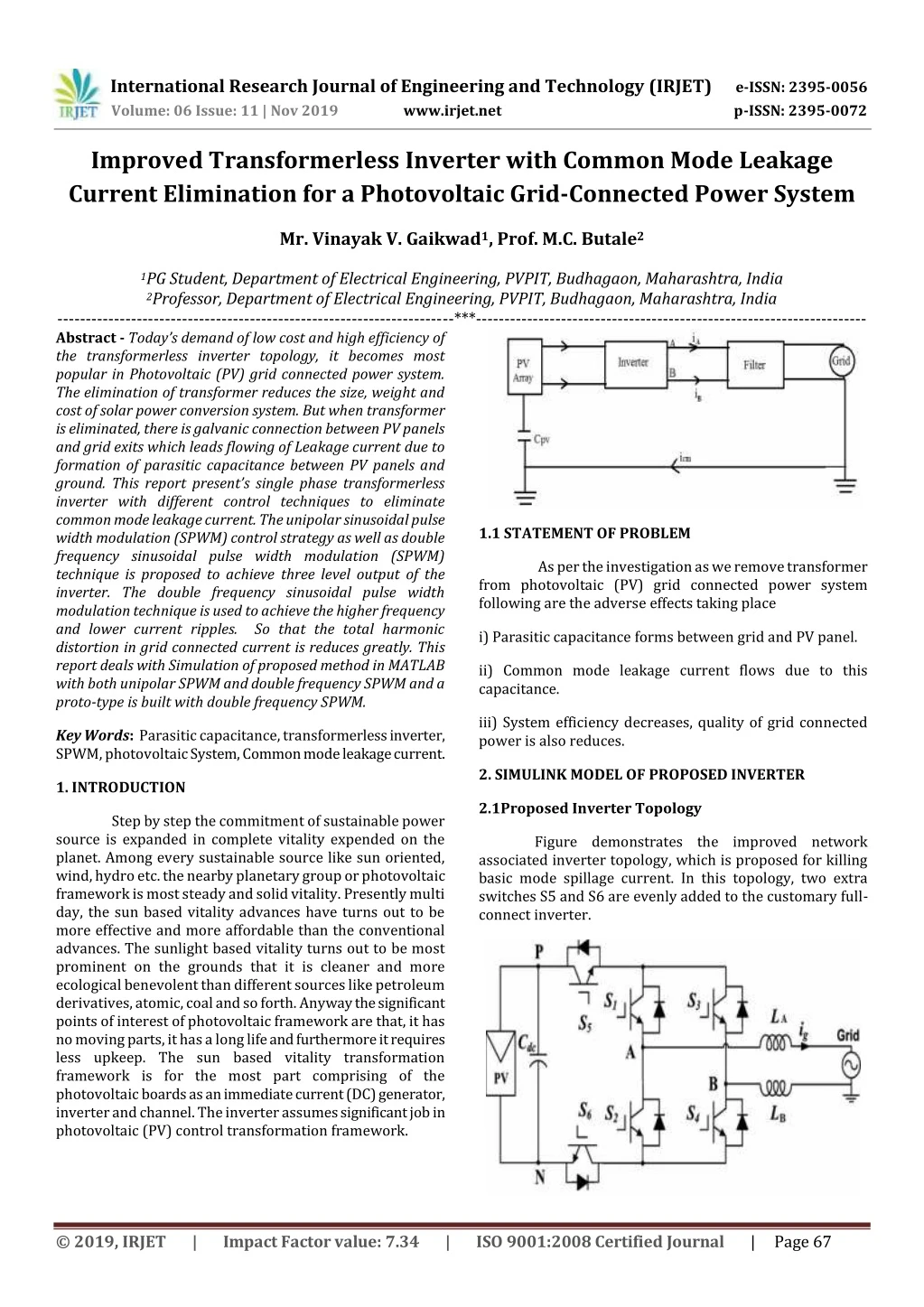
International Research Journal of Engineering and Technology(IRJET) e-ISSN: 2395-0056 Volume: 06 Issue: 11 | Nov 2019 www.irjet.net p-ISSN: 2395-0072 Improved Transformerless Inverter with Common Mode Leakage Current Elimination for a Photovoltaic Grid-Connected Power System Mr. Vinayak V. Gaikwad1, Prof. M.C. Butale2 1PG Student, Department of Electrical Engineering, PVPIT, Budhagaon, Maharashtra, India 2Professor, Department of Electrical Engineering, PVPIT, Budhagaon, Maharashtra, India ----------------------------------------------------------------------***--------------------------------------------------------------------- Abstract -Today’s demand of low cost and high efficiency of the transformerless inverter topology, it becomes most popular in Photovoltaic (PV) grid connected power system. The elimination of transformer reduces the size, weight and cost of solar power conversion system. But when transformer is eliminated, there is galvanic connection between PV panels and grid exits which leads flowing of Leakage current due to formation of parasitic capacitance between PV panels and ground. This report present’s single phase transformerless inverter with different control techniques to eliminate common mode leakage current. The unipolar sinusoidal pulse width modulation (SPWM) control strategy as well as double frequency sinusoidal pulse width modulation (SPWM) technique is proposed to achieve three level output of the inverter. The double frequency sinusoidal pulse width modulation technique is used to achieve the higher frequency and lower current ripples. So that the total harmonic distortion in grid connected current is reduces greatly. This report deals with Simulation of proposed method in MATLAB with both unipolar SPWM and double frequency SPWM and a proto-type is built with double frequency SPWM. 1.1 STATEMENT OF PROBLEM As per the investigation as we remove transformer from photovoltaic (PV) grid connected power system following are the adverse effects taking place i) Parasitic capacitance forms between grid and PV panel. ii) Common mode leakage current flows due to this capacitance. iii) System efficiency decreases, quality of grid connected power is also reduces. Key Words: Parasitic capacitance, transformerless inverter, SPWM, photovoltaic System, Common mode leakage current. 2. SIMULINK MODEL OF PROPOSED INVERTER 1. INTRODUCTION 2.1Proposed Inverter Topology Step by step the commitment of sustainable power source is expanded in complete vitality expended on the planet. Among every sustainable source like sun oriented, wind, hydro etc. the nearby planetary group or photovoltaic framework is most steady and solid vitality. Presently multi day, the sun based vitality advances have turns out to be more effective and more affordable than the conventional advances. The sunlight based vitality turns out to be most prominent on the grounds that it is cleaner and more ecological benevolent than different sources like petroleum derivatives, atomic, coal and so forth. Anyway the significant points of interest of photovoltaic framework are that, it has no moving parts, it has a long life and furthermore it requires less upkeep. The sun based vitality transformation framework is for the most part comprising of the photovoltaic boards as an immediate current (DC) generator, inverter and channel. The inverter assumes significant job in photovoltaic (PV) control transformation framework. Figure demonstrates the improved network associated inverter topology, which is proposed for killing basic mode spillage current. In this topology, two extra switches S5 and S6 are evenly added to the customary full- connect inverter. © 2019, IRJET | Impact Factor value: 7.34 | ISO 9001:2008 Certified Journal | Page 67
International Research Journal of Engineering and Technology(IRJET) e-ISSN: 2395-0056 Volume: 06 Issue: 11 | Nov 2019 www.irjet.net p-ISSN: 2395-0072 2.2Simulink model of proposed transformerless inverter 3.3 Design of L filter: Channel is broadly utilized in power gadgets to diminish consonant parts at the yield waveform. It is likewise utilized for smoothing the voltage wave of a heap nourished from a rectifier in decreasing the symphonious substance of an inverter yield , averting undesirable consonant segment being reflected into AC framework and dispensing with RF interference. Yield of the inverter is a "cleaved DC voltage with zero DC parts". Lf = Therefore, 3. DESIGN AND SPECIFICATIONS Lf = 3.1 Specification = 3.847mH A 1 kW inverter for PV array is simulated to verify the results with considering PV panels are connected to ground by parasitic capacitance. The parameters used for simulating 1 kW inverter are shown in table = 4 mH 4. HARDWEAR DEVELOPMENT 4.1 Block Diagram of the proposed system Parameter Value 1 Kw 380 V 1000 mf 230 Vac 50 Hz 4 Mh 75 Nf Output power Pout Input voltage Vdc Input capacitor Cdc Grid voltage Vg Grid frequency fg Filter inductor Lf Parasitic capacitor Cpv The square chart of the proposed framework is appeared in figure comprises of DC source as an info voltage of the framework, proposed inverter, channel and burden. The proposed inverter incorporates the PIC controller to create SPWM beats, optocoupler utilized for segregation and driver ICs. 3.2 Design of Dc Link Capacitor: The DC connect capacitor is go about as vitality support in inverter and permits stable activity at the MPP. The capacitance required is determined by condition no.32 in which speaks to the ostensible yield control, speaks to the level of the swell on the information voltage, principal recurrence. is the information DC voltage and fg is the matrix 4.2 Design and Specifications A prototype is built which consist of following parameters and specifications, Cdc = Therefore, Parameter Input voltage Vdc Grid frequency fg Switching frequency Filter inductor Lf Load Value 12 V 50 Hz 1 kHz 100 u H 200 KΩ Cdc = = 1102.74 μF = 1000 μF © 2019, IRJET | Impact Factor value: 7.34 | ISO 9001:2008 Certified Journal | Page 68
International Research Journal of Engineering and Technology(IRJET) e-ISSN: 2395-0056 Volume: 06 Issue: 11 | Nov 2019 www.irjet.net p-ISSN: 2395-0072 4.2.1 Design of Crystal Oscillator and capacitors almost certainly obstruct the full voltage found in the particular circuit. A gem oscillator is an electronic circuit that uses the mechanical reverberation of a vibrating precious stone of piezoelectric material to make an electrical sign with an extremely exact recurrence. Quartz gems are made for frequencies from a couple of kilohertz to many megahertz. The PIC16F87XA oscillator configuration requires the utilization of a parallel cut precious stone. Utilization of an arrangement cut gem may give a recurrence out of the precious stone producer's particulars. In this undertaking Crystal Oscillator is utilized to give recurrence to PIC Controller. The base bootstrap capacitor worth can becalculated from the accompanying condition: In this project the value of bootstrapping capacitor is 0.47uf. 4.2.3 Design of current limiting registers for optocoupler The switching frequency required is 1 KHz .Thus the period is, R= T = = = 1 msec. The gem oscillator utilized is of rating 4MHz. Be that as it may, this recurrence of precious stone oscillator is outer recurrence. From this recurrence the working recurrence of PIC controller is determined as, = = 330 ohm 5. CIRCUIT DIAGRAM OF PROPOSED INVERTER 5.1.1 Power supply section F = = 1 MHz. From this frequency period is calculated as, T = = = 1 usec. TMR 1H= 0xFC, TMR 1L= 0x17. Including the capacitance over the precious stone will make the reverberation recurrence decline. For gem oscillator the estimations of capacitors are, CRYSTAL OSCILLATOR AND CAPACITORS VALUES Frequency 455 kHz 2 MHz 4 MHz OSC 1 68-100 pF 15-68 Pf 15-68 Pf OSC 2 68-100 Pf 15-68 pF 15-68 pF 4.2.2 Design of Bootstrapping capacitors for MOSFET Drivers: For the most part, any strategy where part of the yield of a framework is utilized at beginning up is portrayed as bootstrapping. In the area of a MOSFET circuits bootstrapping is generally used to mean pulling a transistor over the power supply. The bootstrap diode and capacitor are the main outside segments carefully required for activity in a standard PWM application. The bootstrap diode must © 2019, IRJET | Impact Factor value: 7.34 | ISO 9001:2008 Certified Journal | Page 69
International Research Journal of Engineering and Technology(IRJET) e-ISSN: 2395-0056 Volume: 06 Issue: 11 | Nov 2019 www.irjet.net p-ISSN: 2395-0072 5.1.2 Microcontroller section 5.1.4 Power Supply: By and by, d.c. control for electronic circuits is most advantageously gotten from business a.c. lines by utilizing rectifier-channel framework, called a d.c. power supply. The rectifier-channel blend establishes a normal d.c. power supply. The d.c. voltage from a customary power supply stays consistent insofar as a.c. mains voltage or burden is unaltered. In any case, in numerous electronic applications, it is wanted that d.c. voltage ought to stay consistent regardless of changes in a.c. mains or burden. Under such circumstances, voltage directing gadgets are utilized with common power supply. This comprises directed d.c. power supply and keeps the d.c. voltage at genuinely steady esteem. The square outline for controlled power supply is appeared in figure 5.1.3 Isolation and Gate drive section 6 SIMULATION RESULTS 6.1 Results under Unipolar SPWM (a) (b) (c) Fig. Simulated results of (a) Output voltage (b) Grid voltage (c) Grid current © 2019, IRJET | Impact Factor value: 7.34 | ISO 9001:2008 Certified Journal | Page 70
International Research Journal of Engineering and Technology(IRJET) e-ISSN: 2395-0056 Volume: 06 Issue: 11 | Nov 2019 www.irjet.net p-ISSN: 2395-0072 Figure (a), (b) and (c) demonstrates the reenacted consequences of inverter yield voltage with three level, matrix voltage and framework associated current for inverter individually under unipolar sinusoidal PWM method. Figure (a), (b) and (c) demonstrates the mimicked consequences of yield voltage with three level, framework voltage and lattice associated current for inverter individually under twofold recurrence sinusoidal PWM system. (a) (a) (b) Fig. Simulated results of (a) common mode voltage (b) common mode leakage current (b) Fig. Simulated results of (a) common mode voltage (b) common mode leakage current 7. HARDWARE RESULTS 6.2 Results under Double frequency SPWM (a) Fig. Waveform of grid voltage (b) Fig. Waveform of grid current (c) Fig. Simulated results of (a) Output voltage (b) Grid voltage (c) Grid current © 2019, IRJET | Impact Factor value: 7.34 | ISO 9001:2008 Certified Journal | Page 71
International Research Journal of Engineering and Technology(IRJET) e-ISSN: 2395-0056 Volume: 06 Issue: 11 | Nov 2019 www.irjet.net p-ISSN: 2395-0072 REFERENCES [1]Q. Li and P. Wolfs, “A review of the single phase photovoltaic module integrated converter topologies with three different DC link configurations” IEEE Trans. Power Electron., vol. 23, no. 3, pp. 1320–1333, May 2008. [2]R. Gonzalez, E. Gubia, J. Lopez, and L. Marroyo, “Transformerless single photovoltaic inverter” IEEE Trans. Ind. Electron., vol. 55, no. 7, pp. 2694–2702, Jul. 2008. phase multilevel-based Fig. Waveforms of grid voltage and grid current. Figure shows the experimental results of grid voltage and grid current of proposed inverter under double frequency SPWM. Figure shows the combine waveforms of grid voltage and grid current of proposed inverter under double frequency SPWM. [3]O. Lopez, F. D. Freijedo, A. G. Yepes, P. Fernandez- Comesaa, J. Malvar, R. Teodorescu, and J. Doval-Gandoy, “Eliminating ground current in a transformerless photovoltaic application” IEEE Trans. Energy Convers., vol. 25, no. 1, pp. 140–147, Mar. 2010. [4]Wenhua Zhu, Shanshui Yang, Li Wang, LingluLuo, Nanjing University of Aeronautics and Astronautics Nanjing, China “Modeling and Analysis of Output Features of the Solar Cells Based on MATLAB/Simulink.” [5]T. Kerekes, R. Teodorescu, and U. Borup, “Transformerless photovoltaic inverters connected to the grid” in Proc. IEEE 22nd Annu. Appl. PowerElectron. Conf., 2007, pp. 1733–1737. [6]G. Vazquez, T. Kerekes, A. Rolan, D. Aguilar, A. Luna, and G. Azevedo,“Losses and transformerless grid-connected PV topologies” in Proc. IEEE Int. Symp. Ind. Electron., Jul. 2009, pp. 544–548. CMV evaluation in Fig. Waveform of common mode leakage current. If the figure which is experimental result is compared with fig. that is simulated result it indicates that the common mode leakage current is completely eliminated in proposed system under double frequency SPWM. [7]T. Kerekes, R. Teodorescu, and M. Liserre, “Common mode voltage in case of transformerless PV inverters connected to the grid” in Proc. IEEEInt. Symp. Ind. Electron., Jun./Jul. 2008, pp. 2390–2395. 8. CONCLUSION The work displayed in this report manages the presentation of proposed transformerless inverter with various control results to accomplish three level yield. The twofold recurrence sinusoidal PWM method accomplishes lower THD in framework associated current than the unipolar sinusoidal PWM procedure. This report likewise introduces the investigation on basic mode spillage current in transformerless inverter and determines that regular mode spillage current is straightforwardly corresponding to change in like manner mode voltage. The mimicked outcomes are demonstrates that as normal mode voltage is kept consistent, the spillage current is totally killed. The equipment result demonstrates that basic mode spillage current is disposed of with Double recurrence SPWM system. 9. FUTURE SCOPE Above simulation and hardware results can be used to develop low cost, low weight, highly efficient transformerless inverters for Photovoltaic grid connected power systems. © 2019, IRJET | Impact Factor value: 7.34 | ISO 9001:2008 Certified Journal | Page 72