Download
1 / 2
20 likes | 27 Views
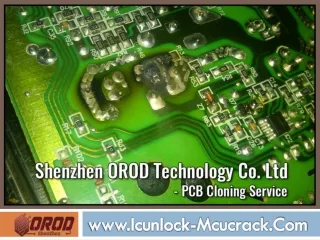
PCB reverse engineering (PCB Copy) is a significant part of PCB design. One of the finest benefits of using printed circuit boards is the amount of time that can be saved. Connecting components conventionally takes a lot of time, whereas the circuit board will take far less time to assemble once the design is total. http://icunlock-mcucrack.com/case/omap4430-based-third-order-hdi-pcb-reverse-engineering

E N D
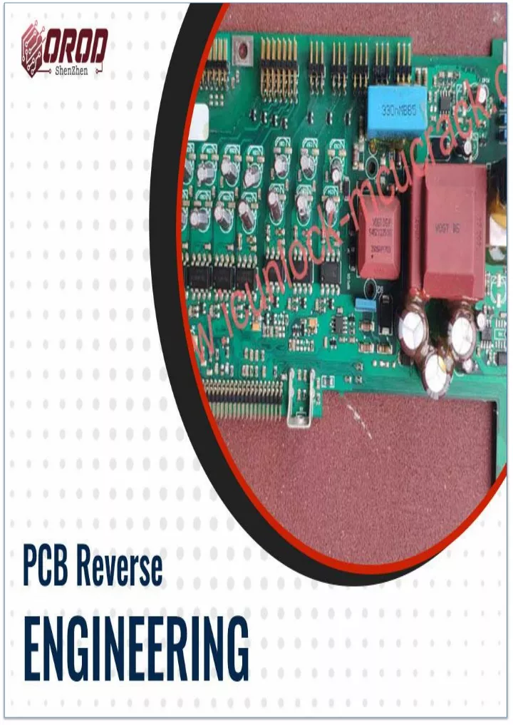
Benefits of PCB reverse engineering PCB copy board is also PCB clone, which is PCB reverse engineeringof design. It is to first withdraw the components on the PCB circuit board to make a BOM list, PCB reverse engineering empty board into a picture, and reinstate it to a pcb board drawing file through the copying software; computing the pcb board drawing file to the PCB board factory to make the board ( PCBA), and then add parts which is exactly the same PCB circuit board as the genuine PCB circuit board. The motive of PCB copy is sometimes to modify the PCB, which is to conduct alter technology research on the designed PCB board. After mention to a lot of information, the process of PCB reverse engineering is outline as follows: The first step is to get a PCB reverseengineering, first record the model, framework, and positions of all crucial parts on paper, especially the direction of the diode, the tertiary tube, and the management of the IC gap. It is best to use a digital camera to take two photos of the location of essential parts. . The secondly detach all the components and take out the tin in the PAD hole. Wash the PCB with alcohol and put it in the scanner. When the scanner scans, you are required to raise the scanned pixels slightly to get a clearer image. Then slowly sand the top and bottom layers with water gauze paper till the copper film is bright, put them in the scanner, start PHOTOSHOP, and scan the two layers individually in colour. China Official headquarters: Address:NO.8536 5th Floor, Bantian Business Building ,Bantian street,Longgang District; City:Shen Zhen; Province/State:Guang Dong Contry:China; Poscode:518129;