Download
1 / 72
840 likes | 1.45k Views
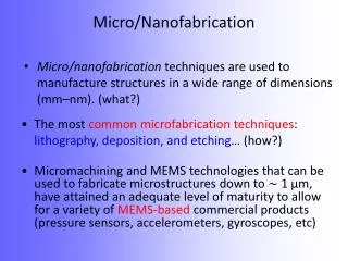
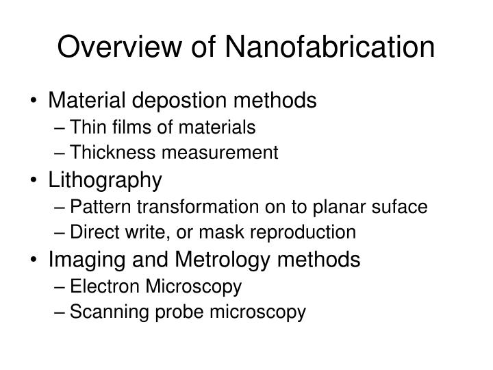
Overview of Nanofabrication. Material depostion methods Thin films of materials Thickness measurement Lithography Pattern transformation on to planar suface Direct write, or mask reproduction Imaging and Metrology methods Electron Microscopy Scanning probe microscopy.

E N D
Overview of Nanofabrication • Material depostion methods • Thin films of materials • Thickness measurement • Lithography • Pattern transformation on to planar suface • Direct write, or mask reproduction • Imaging and Metrology methods • Electron Microscopy • Scanning probe microscopy
Thin film deposition techniques • Vacuum deposition Methods • UHV (<10-8), HV • Sputtering • CVD • Laser Oblation • Thermal deposition • Boat or crucible, E-gun • Epitaxy, growth models
Sputtering substrate Target material B E Ar Vacuum + 10-3 Torr Ar • RF plasma rectifies RF power, gives DC acceleration voltage • Ions circle B field lines, increase colisson probability Ar, N2 RF Power
B Permanent Magnet HV E-gun Filament
Thermal CVD system Precurser Gas For growing Carbon Nanotubes http://www.iljinnanotech.co.kr/en/material/r-4-4.htm
Carbon Nanotubes http://www.iljinnanotech.co.kr/en/material/r-4-4.htm
MBE http://www.wsi.tu-muenchen.de/E24/resources/facilities.htm
The Knudsen Cell (effusion cell) http://www.grc.nasa.gov/WWW/RT2002/5000/5160copland.html
Lithography • Spin coat radiation sensitive polymer - Resist • Expose layer (through mask or direct write) • Develop • Etch away or deposit material
100% Film Retention 0% D2 D1 Resist Contrast Curve Logarithmic measure of slope of contrast curve Negative Resist Positive Resist 100% Film Retention 0% D2 D1
Typical Positive Resist process • EXAMPLE PROCESS: AZ5206 POSITIVE MASK PLATE • Soak mask plate in acetone > 10 min to remove the original photoresist. • Rinse in isopropanol, blow dry. • Clean the plate with RIE in oxygen. Do not use a barrel etcher. • RIE conditions: 30 sccm O2, 30 mTorr total pressure, 90 W (0.25 W/cm2), 5 min. • Immediately spin AZ5206, 3 krpm. • Bake at 80 C for 30 min. • Expose with e-beam, 10 kV, 6 C/cm2, Make sure the plate is well grounded. • (Other accelerating voltages may be used, but the dose will be different.) • Develop for 60 s in KLK PPD 401 developer. Rinse in water. • Descum - important Same as step 2 above, for only 5 seconds • Or use a barrel etcher, 0.6 Torr oxygen, 150W, 1 min. • If this is a Cr plate, etch with Transene Cr etchant, ~1.5 min. • If this is a MoSi plate, then RIE etch: • 0.05 Torr total pressure, 0.05 W/cm2, 16 sccm SF6, 4.2 sccm CF4,1 min. • Plasma clean to remove resist: same as step 2 above, for 3 min.
Typical Negative resist process • EXAMPLE PROCESS: SAL NEGATIVE MASK PLATE • Soak mask plate in acetone > 10 min to remove photoresist. • Clean the plate with RIE in oxygen. Do not use a barrel etcher. • RIE conditions: 30 sccm O2, 30 mTorr total pressure, 90 W (0.25 W/cm2), 5 min. • Immediately spin SAL-601, 4 krpm, 1 min. • Bake in 90 C oven for 10 min. This resist is not sensitive to room light. • Expose at 50 kV, 11 C/cm2. Be sure the plate is grounded. • Post-bake for 1 min on a large hotplate, 115 C. • Cool for > 6 min. • Develop for 6 min in Shipley MF312:water (1:1) Be sure to check for underdevelopment. • Descum 30 s with oxygen RIE: same as step 2, 10 s. • Etch with Transene or Cyantek Cr etchant, ~1.5 min. • Plasma clean to remove resist: Same as step 2, 5 min.
Photo Lithography • Project UV light through Mask • Non contact with optical reduction (typical 4X) • Contact with one-to-one pattern transfer • Mask – very flat SiO2 plate with Cr thin film • Resolution limited by wave length (phase shift) • Optics hard for short wave lengths
Electron Beam Lithograpy • Literature, Resources • Handbook of Microlithography Micromachining and Microfabrication, ed. P. Rai-Choudhury, SPEI press (chapter two is on the web, linked from home page • J C Nabity web site: http://www.jcnabity.com • Course material is posted on web site in restricted area: • http://www.nanophys.kth.se education Intro. to e-beam Lithography • Link to restricted area (password protected) Username: ebeamlecture Password: lithogr
Some things you can do with EBL Circuit of SQUIDs and Josephson Tunnel Junctions
1.5 mm Bonding Pads Contact “cage” to nano-circuit -- for rapid testing
Connecting Strips
Ferromagnetic - Normal metal tunnel junctions Co 100 nm Al Circuit to measure spin injection from ferromagnet (Co) to normal metal (Al)
Innerdigitated Capacitor in coplanar waveguide Cooper Pair Transistor
All these structure were made with one layer of e-beam lithography and one vacuum deposition cycle!
Aperture Lens a – convergence angle Electron Optics detector sample Scanning the electron beam
Electron scattering limits resolution Higher energy electrons have larger back-scattering range
Overview of systems • SEM conversion (NPGS) • SEM modification (Raith) • High end system • SEM conversion limited in speed by slow beam deflection system (induction in magnet coils). • Laser stage is big step in price, but necessary for accurate pattern writing and stitching. • The more complex the system, the more service and higher user costs • Industry Fab. machines not always well suited to research needs.
NPGS • Joe Nabity, one man company, good reputation, very helpful, good support • Works with many SEMS • Can do stage control, many SEMs come with micrometer, motor control (accuracy) • Can do precision alignment in single field by scanning in reduced area to find mark. Manual mark detection. Good Web site: http://www.jcnabity.com list of references, pictures, ideas
Fabricated with NPGS This image shows a pattern of radially placed dots in PMMA after development. The white bar at the bottom of the image is 1 micron long. The pattern was designed as radial lines, but the spacing of the exposure points was set 0.3 microns to produce discrete dots. Notice how the dot size and spacing is very consistent in all directions. The exposure was done with an SEM with no beam blanker and the image was taken with the NPGS digital imaging feature. The pattern was written by Dr. ChiiDong Chen at the Institute of Physics, Academia Sinica, Taiwan. This picture shows part of a circular grating with a period of 0.15 microns. The lines appear almost straight, because they are near the outer edge of the grating where the radius is ~100 microns. The pattern was written in PMMA and has been coated with gold for viewing. The lithography was done at the Optical Sciences Center at the University of Arizona.
L= 80 nm 50 nm 30 nm 25 nm 18 nm 16 nm 20 nm 15 nm Proven resolution with our Raith 150 courtesy of Anders Holmberg L=Line width (pitch = 2L)
Nanophys positive process for one-cycle tunnel junction fabrication • Two layer resist, selective developers • Very large undercut – suspended bridge • Tunnel junction (top and base layer) in one layer Top view of pattern Exposed areas Undercut region Supporting resist Next slides: Cut on this axis
Lithography and shadow evaporation ZEP 520 PMGI SF7 SiOx Si
Irradiate with electron beam Lithography and shadow evaporation
Develop the two layers selectively Top layer: Bottom Layer: Lithography and shadow evaporation
Lithography and shadow evaporation Evaporate Al at an angle
Lithography and shadow evaporation Oxidize the first layer
Lithography and shadow evaporation Evaporate Al at opposite angle
Lithography and shadow evaporation Lift off the resist and excess metal Tunnel junctions
Voilà Circuit of SQUIDs and Josephson Tunnel Junctions
3D structuring using contrast curve • Accurately measure thickness of film • Do test pattern with dose profile to accurately measure contrast curve
Patterning in third dimension Desired structure: thickness Dose
Holography Positive electron resist SAL 110 Developer SAL 101 (Shipley) Chalmers Group, S. Hård et al. Applied Optics vol. 33 p 1176, 1994
Optical Kinoforms Chalmers Group, S. Hård et al. Applied Optics vol. 33 p 1176, 1994 Optical Comm. Vol. 88, p 37, 1992