Download
1 / 30
300 likes | 312 Views
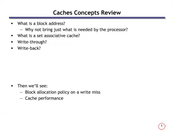
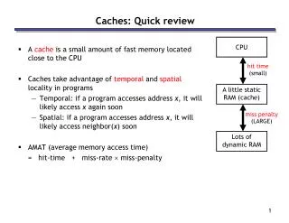
Caches Concepts Review. What is a block address? Why not bring just what is needed by the processor? What is a set associative cache? Write-through? Write-back? Then we’ll see: Block allocation policy on a write miss Cache performance. Byte Address. Block Address. 0 1 2 3 4 5 6

E N D
Caches Concepts Review • What is a block address? • Why not bring just what is needed by the processor? • What is a set associative cache? • Write-through? • Write-back? • Then we’ll see: • Block allocation policy on a write miss • Cache performance
Byte Address Block Address 0 1 2 3 4 5 6 7 8 9 10 11 12 13 14 15 0 1 2 3 4 5 6 7 Block addresses • Now how can we figure out where data should be placed in the cache? • It’s time for block addresses! If the cache block size is 2n bytes, we can conceptually split the main memory into 2n-byte chunks too. • To determine the block address of a byte address i, you can do the integer division i / 2n • Our example has two-byte cache blocks, so we can think of a 16-byte main memory as an “8-block” main memory instead. • For instance, memory addresses 12 and 13 both correspond to block address 6, since 12 / 2 = 6 and 13 / 2 = 6.
8-way 1 set, 8 blocks 1-way 8 sets, 1 block each 2-way 4 sets, 2 blocks each 4-way 2 sets, 4 blocks each Set Set Set Set 0 1 2 3 4 5 6 7 0 1 2 3 0 1 0 direct mapped fully associative Set associative caches are a general idea • By now you may have noticed the 1-way set associative cache is the same as a direct-mapped cache. • Similarly, if a cache has 2k blocks, a 2k-way set associative cache would be the same as a fully-associative cache.
Mem[214] = 21763 Index V Tag Data Address Data ... 110 ... ... 1101 0110 ... 1 11010 21763 21763 Write-through caches • A write-through cache forces all writes to update both the cache and the main memory. • This is simple to implement and keeps the cache and memory consistent. • The bad thing is that forcing every write to go to main memory, we use up bandwidth between the cache and the memory.
Write-back caches • In a write-back cache, the memory is not updated until the cache block needs to be replaced (e.g., when loading data into a full cache set). • For example, we might write some data to the cache at first, leaving it inconsistent with the main memory as shown before. • The cache block is marked “dirty” to indicate this inconsistency • Subsequent reads to the same memory address? • Multiple writes to same block? Mem[214] = 21763 Index V Dirty Tag Data Address Data ... 110 ... 1000 1110 1101 0110 ... 1225 1 1 11010 21763 42803
Write-back cache discussion • The advantage of write-back caches is that not all write operations need to access main memory, as with write-through caches. • If a single address is frequently written to, then it doesn’t pay to keep writing that data through to main memory. • If several bytes within the same cache block are modified, they will only force one memory write operation at write-back time.
Index V Tag Data Address Data ... 110 ... ... 1101 0110 ... 1 00010 123456 6378 Write misses • A second scenario is if we try to write to an address that is not already contained in the cache; this is called a write miss. • Let’s say we want to store 21763 into Mem[1101 0110] but we find that address is not currently in the cache. • When we update Mem[1101 0110], should we also load it into the cache?
Mem[214] = 21763 Address Data Index V Tag Data ... 1101 0110 ... ... 110 ... 21763 1 00010 123456 Write around caches (a.k.a. write-no-allocate) • With a write around policy, the write operation goes directly to main memory without affecting the cache.
Mem[214] = 21763 Address Data Index V Tag Data ... 1101 0110 ... ... 110 ... 21763 1 00010 123456 Write around caches (a.k.a. write-no-allocate) • With a write around policy, the write operation goes directly to main memory without affecting the cache. • This is good when data is written but not immediately used again, in which case there’s no point to load it into the cache yet. for (int i = 0; i < SIZE; i++) a[i] = i;
Mem[214] = 21763 Index V Tag Data Address Data ... 110 ... ... 1101 0110 ... 1 11010 21763 21763 Allocate on write • An allocate on write strategy would instead load the newly written data into the cache. • If that data is needed again soon, it will be available in the cache.
Which is it? • Given the following trace of accesses, can you determine whether the cache is write-allocate or write-no-allocate? • Assume A and B are distinct, and can be in the cache simultaneously. Miss Load A Miss Store B Hit Store A Hit Load A Miss Load B Hit Load B Hit Load A
Which is it? • Given the following trace of accesses, can you determine whether the cache is write-allocate or write-no-allocate? • Assume A and B are distinct, and can be in the cache simultaneously. Miss Load A Miss Store B Hit Store A Hit Load A Miss Load B Hit Load B Hit Load A On a write-allocate cache this would be a hit Answer: Write-no-allocate
Main Memory L2 cache CPU L1 cache First Observations • Split Instruction/Data caches: • Pro: No structural hazard between IF & MEM stages • A single-ported unified cache stalls fetch during load or store • Con: Static partitioning of cache between instructions & data • Bad if working sets unequal: e.g.,code/DATA or CODE/data • Cache Hierarchies: • Trade-off between access time & hit rate • L1 cache can focus on fast access time (okay hit rate) • L2 cache can focus on good hit rate (okay access time) • Such hierarchical design is another “big idea”
Main Memory L2 cache CPU L1 cache Opteron Vital Statistics • L1 Caches: Instruction & Data • 64 kB • 64 byte blocks • 2-way set associative • 2 cycle access time • L2 Cache: • 1 MB • 64 byte blocks • 4-way set associative • 16 cycle access time (total, not just miss penalty) • Memory • 200+ cycle access time
Comparing cache organizations • Like many architectural features, caches are evaluated experimentally. • As always, performance depends on the actual instruction mix, since different programs will have different memory access patterns. • Simulating or executing real applications is the most accurate way to measure performance characteristics. • The graphs on the next few slides illustrate the simulated miss rates for several different cache designs. • Again lower miss rates are generally better, but remember that the miss rate is just one component of average memory access time and execution time.
12% 9% Miss rate 6% 3% 0% One-way Two-way Four-way Eight-way Associativity Associativity tradeoffs and miss rates • As we saw last time, higher associativity means more complex hardware. • But a highly-associative cache will also exhibit a lower miss rate. • Each set has more blocks, so there’s less chance of a conflict between two addresses which both belong in the same set. • Overall, this will reduce AMAT and memory stall cycles. • The textbook shows the miss rates decreasing as the associativity increases.
15% 12% 9% 1 KB Miss rate 2 KB 4 KB 6% 8 KB 3% 0% One-way Two-way Four-way Eight-way Associativity Cache size and miss rates • The cache size also has a significant impact on performance. • The larger a cache is, the less chance there will be of a conflict. • Again this means the miss rate decreases, so the AMAT and number of memory stall cycles also decrease. • The complete Figure 7.30 depicts the miss rate as a function of both the cache size and its associativity.
40% 35% 30% 1 KB 25% 8 KB 20% Miss rate 16 KB 64 KB 15% 10% 5% 0% 4 16 64 256 Block size (bytes) Block size and miss rates • Miss rates relative to the block size and overall cache size. • Smaller blocks do not take maximum advantage of spatial locality.
Memory and overall performance • How do cache hits and misses affect overall system performance? • Assuming a hit time of one CPU clock cycle, program execution will continue normally on a cache hit. (Our earlier computations always assumed one clock cycle for an instruction fetch or data access.) • For cache misses, we’ll assume the CPU must stall to wait for a load from main memory. • The total number of stall cycles depends on the number of cache misses and the miss penalty. Memory stall cycles = Memory accesses x miss rate x miss penalty • To include stalls due to cache misses in CPU performance equations, we have to add them to the “base” number of execution cycles. CPU time = (CPU execution cycles + Memory stall cycles) x Cycle time
Performance example • Assume that 33% of the instructions in a program are data accesses. The cache hit ratio is 97% and the hit time is one cycle, but the miss penalty is 20 cycles. Memory stall cycles = Memory accesses x Miss rate x Miss penalty = 0.33 I x 0.03 x 20 cycles = 0.2 I cycles • If I instructions are executed, then the number of wasted cycles will be 0.2 x I. This code is 1.2 times slower than a program with a “perfect” CPI of 1!
Memory systems are a bottleneck CPU time = (CPU execution cycles + Memory stall cycles) x Cycle time • Processor performance traditionally outpaces memory performance, so the memory system is often the system bottleneck. • For example, with a base CPI of 1, the CPU time from the last page is: CPU time = (I + 0.2 I) x Cycle time • What if we could double the CPU performance so the CPI becomes 0.5, but memory performance remained the same? CPU time = (0.5 I + 0.2 I) x Cycle time • The overall CPU time improves by just 1.2/0.7 = 1.7 times! • Refer back to Amdahl’s Law. • Speeding up only part of a system has diminishing returns.
CPU Cache Main Memory Basic main memory design • There are some ways the main memory can be organized to reduce miss penalties and help with caching. • For some concrete examples, let’s assume the following three steps are taken when a cache needs to load data from the main memory. • It takes 1 cycle to send an address to the RAM. • There is a 15-cycle latency for each RAM access. • It takes 1 cycle to return data from the RAM. • In the setup shown here, the buses from the CPU to the cache and from the cache to RAM are all one word wide. • If the cache has one-word blocks, then filling a block from RAM (i.e., the miss penalty) would take 17 cycles. 1 + 15 + 1 = 17 clock cycles • The cache controller has to send the desired address to the RAM, wait and receive the data.
CPU Cache Main Memory Miss penalties for larger cache blocks • If the cache has four-word blocks, then loading a single block would need four individual main memory accesses, and a miss penalty of 68 cycles! 4 x (1 + 15 + 1) = 68 clock cycles
CPU Cache Main Memory A wider memory • A simple way to decrease the miss penalty is to widen the memory and its interface to the cache, so we can read multiple words from RAM in one shot. • If we could read four words from the memory at once, a four-word cache load would need just 17 cycles. 1 + 15 + 1 = 17 cycles • The disadvantage is the cost of the wider buses—each additional bit of memory width requires another connection to the cache.
CPU Cache Main Memory Bank 0 Bank 1 Bank 2 Bank 3 An interleaved memory • Another approach is to interleave the memory, or split it into “banks” that can be accessed individually. • The main benefit is overlapping the latencies of accessing each word. • For example, if our main memory has four banks, each one word wide, then we could load four words into a cache block in just 20 cycles. 1 + 15 + (4 x 1) = 20 cycles • Our buses are still one word wide here, so four cycles are needed to transfer data to the caches. • This is cheaper than implementing a four-word bus, but not too much slower.
Clock cycles Load word 1 Load word 2 Load word 3 Load word 4 15 cycles Interleaved memory accesses • Here is a diagram to show how the memory accesses can be interleaved. • The magenta cycles represent sending an address to a memory bank. • Each memory bank has a 15-cycle latency, and it takes another cycle (shown in blue) to return data from the memory. • This is the same basic idea as pipelining! • As soon as we request data from one memory bank, we can go ahead and request data from another bank as well. • Each individual load takes 17 clock cycles, but four overlapped loads require just 20 cycles.
Which is better? • Increasing block size can improve hit rate (due to spatial locality), but transfer time increases. Which cache configuration would be better? • Assume both caches have single cycle hit times. Memory accesses take 15 cycles, and the memory bus is 8-bytes wide: • i.e., an 16-byte memory access takes 18 cycles: 1 (send address) + 15 (memory access) + 2 (two 8-byte transfers) recall: AMAT = Hit time + (Miss rate x Miss penalty)
Which is better? • Increasing block size can improve hit rate (due to spatial locality), but transfer time increases. Which cache configuration would be better? • Assume both caches have single cycle hit times. Memory accesses take 15 cycles, and the memory bus is 8-bytes wide: • i.e., an 16-byte memory access takes 18 cycles: 1 (send address) + 15 (memory access) + 2 (two 8-byte transfers) recall: AMAT = Hit time + (Miss rate x Miss penalty) Cache #1: Miss Penalty = 1 + 15 + 32B/8B = 20 cycles AMAT = 1 + (.05 * 20) = 2 Cache #2: Miss Penalty = 1 + 15 + 64B/8B = 24 cycles AMAT = 1 + (.04 * 24) = ~1.96
Summary • Writing to a cache poses a couple of interesting issues. • Write-through and write-back policies keep the cache consistent with main memory in different ways for write hits. • Write-around and allocate-on-write are two strategies to handle write misses, differing in whether updated data is loaded into the cache. • Memory system performance depends upon the cache hit time, miss rate and miss penalty, as well as the actual program being executed. • We can use these numbers to find the average memory access time. • We can also revise our CPU time formula to include stall cycles. AMAT = Hit time + (Miss rate x Miss penalty) Memory stall cycles = Memory accesses x miss rate x miss penalty CPU time = (CPU execution cycles + Memory stall cycles) x Cycle time • The organization of a memory system affects its performance. • The cache size, block size, and associativity affect the miss rate. • We can organize the main memory to help reduce miss penalties. For example, interleaved memory supports pipelined data accesses.
Writing Cache Friendly Code • Two major rules: • Repeated references to data are good (temporal locality) • Stride-1 reference patterns are good (spatial locality) • Example: cold cache, 4-byte words, 4-word cache blocks int sum_array_rows(int a[M][N]) { int i, j, sum = 0; for (i = 0; i < M; i++) for (j = 0; j < N; j++) sum += a[i][j]; return sum; } int sum_array_cols(int a[M][N]) { int i, j, sum = 0; for (j = 0; j < N; j++) for (i = 0; i < M; i++) sum += a[i][j]; return sum; } Miss rate = Miss rate = 100% 1/4 = 25% Adapted from Randy Bryant