Download
1 / 23
270 likes | 609 Views
Logic Families. Introduction. Logic Family Definition. A circuit configuration or approach used to produce a type of digital integrated circuit.

E N D
Logic Families Introduction
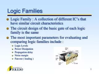
Logic Family Definition • A circuit configuration or approach used to produce a type of digital integrated circuit. • Consequence: different logic functions, when fabricated in the form of an IC with the same approach, or in other words belonging to the same logic family, will have identical electrical characteristics. • the set of digital ICs belonging to the same logic family are electrically compatible with each other
Common Characteristics of the Same Logic Family • Supply voltage range, speed of response, power dissipation, input and output logic levels, current sourcing and sinking capability, fan-out, noise margin, etc. • Consequence: choosing digital ICs from the same logic family guarantees that these ICs are compatible with respect to each other and that the system as a whole performs the intended logic function.
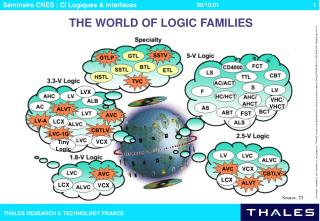
Types of Logic Family 1 • The entire range of digital ICs is fabricated using either bipolar devices or MOS devices or a combination of the two. • Bipolar families: • Diode logic (DL). (obsolete) • Resistor transistor logic (RTL). (obsolete) • Diode transistor logic (DTL). (obsolete) • Transistor Transistor logic (TTL). • Emitter Coupled Logic (ECL), also known as Current Mode Logic(CML). • Integrated Injection logic (I2L). (obsolete)
Types of Logic Family 2 • MOS families: • PMOS family (using P-channel MOSFETs) • The NMOS family (using N-channel MOSFETs) • The CMOS family (using both N- and P-channel devices). • The Bi-MOS logic family uses both bipolar and MOS devices.
CMOS Sub families • 4000A • 4000B, 4000UB, • 54/74C, 54/74HC, 54/74HCT, 54/74AC and 54/74ACT(TTL pin compatible)
Characteristic Parameters 1 • HIGH-level input current, IIH (current flowing into (taken as positive) or out of (taken as negative) an input when a HIGH-level input voltage equal to the minimum HIGH-level output voltage specified for the family is applied. • LOW-level input current, IIL. is the maximum current flowing into (taken as positive) or out of (taken as negative) the input of a logic function when the voltage applied at the input equals the maximum LOW-level output voltage specified for the family. • unit load (UL) HIGH-level and LOW-level input current or loading typically found in data sheets (For devices of the TTL family, 1 UL (HIGH)=40 A and 1 UL (LOW)=1.6 mA.
Characteristic Parameters 2 • HIGH-level output current, IOH.This is the maximum current flowing out of an output when the input conditions are such that the output is in the logic HIGH state. Typically negative number. • LOW-level output current, IOL. This is the maximum current flowing into the output pin of a logic function when the input conditions are such that the output is in the logic LOW state.
Characteristic Parameters 3 • HIGH-level off-state (high-impedance state) output current, IOZH. This is the current flowinginto an output of a tristate logic function with the ENABLE input chosen so as to establish a high-impedance state and a logic HIGH voltage level applied at the output. The input conditions are chosen so as to produce logic LOW if the device is enabled.
Characteristic Parameters 4 • LOW-level input voltage, VIL.This is the maximum voltage level applied at the input that is recognized as a legal LOW level for the specified family. • HIGH-level output voltage, VOH.This is the minimum voltage on the output pin of a logic functionwhen the input conditions establish logic HIGH at the output for the specified family.
Characteristic Parameters 5 • HIGH-level output voltage, VOH.This is the minimum voltage on the output pin of a logic functionwhen the input conditions establish logic HIGH at the output for the specified family.
Characteristic Parameters 6 • Supply current, ICC. The supply current when the output is HIGH, LOW and in the high-impedancestate is respectively designated as ICCH, ICCL and ICCZ. • Rise time, tr. This is the time that elapses between 10 and 90 % of the final signal level when thesignal is making a transition from logic LOW to logic HIGH. • Fall time, tf. This is the time that elapses between 90 and 10 % of the signal level when it is makingHIGH to LOW transition.
Characteristic Parameters 7 • Propagation delay tp. is the time delay between the occurrence of change in the logical level at the input and before it is reflected at the output. It is the time delay between the specified voltage points on the input and output waveforms. • Propagation delays are separately defined for LOW-to-HIGH and HIGH-to-LOW transitions at the output. In addition, we also define enable and disable time delays that occur during transition between the high-impedance state and defined logic LOW or HIGH states.
Characteristic Parameters 8 • Maximum clock frequency, fmax.This is the maximum frequency at which the clock input of aflip-flop can be driven through its required sequence while maintaining stable transitions of logic level at the output in accordance with the input conditions and the product specification. • Power dissipation.The power dissipation parameter for a logic family is specified in terms ofpower consumption per gate and is the product of supply voltage VCC and supply current ICC.
Characteristic Parameters 9 • Speed–power product.The speed of a logic circuit can be increased, that is, the propagation delaycan be reduced, at the expense of power dissipation. • Fan-out. is the number of inputs of a logic function that can be driven from a single output without causing any false output. • Noise margin. This is a quantitative measure of noise immunity offered by the logic family. Whenthe output of a logic device feeds the input of another device of the same family, a legal HIGH logic state at the output of the feeding device should be treated as a legal HIGH logic state by the input of the device being fed. Similarly, a legal LOW logic state of the feeding device should be treated as a legal LOW logic state by the device being fed.