1 / 63

Figure 14.2 Input and output logic levels for CMOS.

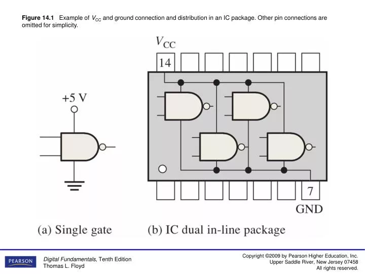
Figure 14.1 Example of V CC and ground connection and distribution in an IC package. Other pin connections are omitted for simplicity. Figure 14.2 Input and output logic levels for CMOS. Figure 14.3 Input and output logic levels for TTL.

aliza
Download Presentation

Figure 14.2 Input and output logic levels for CMOS.

An Image/Link below is provided (as is) to download presentation Download Policy: Content on the Website is provided to you AS IS for your information and personal use and may not be sold / licensed / shared on other websites without getting consent from its author. Content is provided to you AS IS for your information and personal use only. Download presentation by click this link. While downloading, if for some reason you are not able to download a presentation, the publisher may have deleted the file from their server. During download, if you can't get a presentation, the file might be deleted by the publisher.

E N D

Presentation Transcript


  1. Figure 14.1 Example of VCC and ground connection and distribution in an IC package. Other pin connections are omitted for simplicity.

  2. Figure 14.2 Input and output logic levels for CMOS.

  3. Figure 14.3 Input and output logic levels for TTL.

  4. Figure 14.4 Illustration of the effects of input noise on gate operation.

  5. Figure 14.5 Illustration of noise margins. Values are for 5 V CMOS, but the principle applies to any logic family.

  6. Figure 14.6 Currents from the dc supply. Conventional current direction is shown. Electron flow notation is opposite.

  7. Figure 14.7 Power-versus-frequency curves for TTL and CMOS.

  8. Figure 14.8 A basic illustration of propagation delay time.

  9. Figure 14.9 Propagation delay times.

  10. Figure 14.10 Loading a gate output with gate inputs.

  11. Figure 14.11 Capacitive loading of a CMOS gate.

  12. Figure 14.12 Basic illustration of current sourcing and current sinking in logic gates.

  13. Figure 14.13 HIGH-state TTL loading.

  14. Figure 14.14 LOW-stage TTL loading.

  15. Figure 14.15 Basic symbols and switching action of MOSFETs.

  16. Figure 14.16 Simplified MOSFET symbol.

  17. Figure 14.17 A CMOS inverter circuit.

  18. Figure 14.18 Operation of a CMOS inverter.

  19. Figure 14.19 A CMOS NAND gate circuit.

  20. Figure 14.20 A CMOS NOR gate circuit.

  21. Figure 14.21 Open-drain CMOS gates.

  22. Figure 14.22 The three states of a tristate circuit.

  23. Figure 14.23 A tristate CMOS inverter.

  24. Figure 14.24 Handling unused CMOS inputs.

  25. Figure 14.25 The symbol for a BJT.

  26. Figure 14.26 The ideal switching action of the BJT. Conventional current direction is shown. Electron flow notationis opposite.

  27. Figure 14.27 A standard TTL inverter circuit.

  28. Figure 14.28 Operation of a TTL inverter.

  29. Figure 14.29 A TTL NAND gate circuit.

  30. Figure 14.30 Diode equivalent of a TTL multiple-emitter transistor.

  31. Figure 14.31 TTL inverter with open-collector output.

  32. Figure 14.32 Open-collector symbol in an inverter.

  33. Figure 14.33 Basic tristate inverter circuit.

  34. Figure 14.34 An equivalent circuit for the tristate output in the high-Z state.

  35. Figure 14.35 Schottky TTL NAND gate.

  36. Figure 14.36 Current sinking and sourcing action in TTL.

  37. Figure 14.37 A wired-AND configuration of four inverters.

  38. Figure 14.38 Open-collector wired negative-AND operation with inverters.

  39. Figure 14.39

  40. Figure 14.40

  41. Figure 14.41 Totem-pole outputs wired together. Such a connection may cause excessive current through Q1 of device A and Q2 of device B and should never be used.

  42. Figure 14.42 Some applications of open-collector drivers.

  43. Figure 14.43

  44. Figure 14.44 Comparison of an open TTL input and a HIGH-level input.

  45. Figure 14.45 Methods for handling unused TTL inputs.

  46. Figure 14.46 An ECL OR/NOR gate circuit.

  47. Figure 14.47 Basic PMOS gate.

  48. Figure 14.48 Two NMOS gates.

  49. Figure 14.49 An E2CMOS cell.

  50. Figure 14.50

More Related