Download
1 / 22
220 likes | 373 Views
System Architecture of Detector Control and Safety for the ATLAS Inner Detector Upgrade. Didier Ferrère , DPNC Université de Genève. Susanne Kersten, Wuppertal University. New Inner Detector for ATLAS Upgrade. Under consideration:

E N D
System Architecture of Detector Control and Safety for the ATLAS Inner Detector Upgrade Didier Ferrère, DPNC Université de Genève Susanne Kersten, Wuppertal University
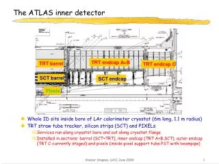
New Inner Detector for ATLAS Upgrade • Under consideration: • Current silicon tracker is expected to smoothly die with an integrated luminosity (< 600 fb-1) : Radiation damages and Inefficiencies at high rate. • A new ID is foreseen at phase 2 Upgrade of the machine and for data taking in ~2020 • The electrical services between the counting rooms and the cavern remain a constraint for the new detector • All the hardware for the FE electronics, the DAQ, the power supply and the DCS will have to be renewed • The cooling is one of the critical challenges for the future silicon tracker with requested operational temperature down to -40°C • All the development has to fit in the framework of the existing ATLAS DAQ, DCS, Trigger with some restrictions under study One ID layout under consideration 4 pixel layers 3 Short-strip layers 2 Long-strip layers 2 D. Ferrère HSTD7, Aug 29th Sept 1st, 2009 in Hiroshima
Pixel & Strip to be renewed Cooling and ID environment to be renewed ATLAS Detector Control System to be Updated The new DCS structure has to fit in the ATLAS GCS 3 D. Ferrère HSTD7, Aug 29th Sept 1st, 2009 in Hiroshima
DCS Motivations Up to 180 kW to control and monitor during the operation in term of power, cooling, and environment across the all ID. The DCS has to be defined as early as possible such it is integrated into the readout architecture together with the powering and the services. • Towards the specifications: • Define the needs Use cases (close to current tracker) • The detector safety and the interlock to be considered as the 1st requirement • Monitoring sources to be well evaluated • Minimize as much as possible the material and the services • Optimize the development effort • Limit access installation in the cavern DCS hardware in the counting room • Try to define a common Pixel and Strip DCS architecture if possible • Search for adequate sensors: Humidity, others? • Identify all the topics where early resources may be necessary • Define the prototypes for DCS investigations like power monitoring and control 4 D. Ferrère HSTD7, Aug 29th Sept 1st, 2009 in Hiroshima
Cooling In Module #1 Module #2 Module #12 TTC, Data & DCS fibers Opto GBT DCS interlock DCS env. IN Cooling Out SMC Hybrid MCC MCC MCC MCC MCC MCC Service bus PS cable Beam Axis IP * the GBT (Giga Bit Transmission) is a chip for data transmission developed by the CERN PH-ESE group Short Strip Barrel Stave Layout • Comments: • SMC is located at the stave end and steer 24 hybrids. In total and per stave there are 2 SMCs: one per side. • SMC (Super Module Controller) is a hybrid board which integrates the opto, the GBT, the DCS and some power regulations • 1 or 2 MCC (Module Controller Chip) steer the data of the 20 chips on a hybrid • The service bus is running below the Si-wafers and the front and back detector bias are separated. • There are 2 SMCs par Stave/SM electrically separated from the top and bottom side 5 D. Ferrère HSTD7, Aug 29th Sept 1st, 2009 in Hiroshima
FE FE FE FE FE FE FE FE FE FE FE FE FE FE FE FE Pixel Barrel Stave Layout 2 single sided staves sandwiched together back to back Module 7 Module 0 End of Stave Card FE FE FE FE FE FE FE FE FE FE FE FE FE FE FE FE DCS GBT* GBT* DCS half stave Beam Axis IP * the GBT (Giga Bit Transmission) is a chip for data transmission developed by the CERN PH-ESE group • Comments: • The construction of the staves varies between the different layers 24 - 32 modules/stave • There are 4 Front End chips/detector module • The DCS relevant building blocks are half stave/disk sector: up to 16 modules + 1 EoS card • For both Pixel and strip two options are considered for the powering: • - Serial powering • - Parallel powering with 2 DC-DC stages 6 D. Ferrère HSTD7, Aug 29th Sept 1st, 2009 in Hiroshima
ID DCS Not defined yet! Cool DCS ID DCS Gen? Strip DCS Pixel DCS Strip Stave Env DCS Power Supply Pixel Stave Env DCS at PS Elect. Opto Elect. Opto Elect. DCS at PS Lines from staves to counting room SPI or I2C DCS split at BOC/ROD @ PS card DCS Data with RO Data DCS Data with RO Data or DCS Chip @ « BBIM » FE DCS DCS Chip FE DCS Lines from staves to counting room @ « BBIM » @ « SMC » ‘SMC Interlock’ @ « BBIM » ‘Cooling Interlock’ ‘Strip Module Interlock’ ‘Pixel Module Interlock’ ID Upgrade DCS Architecture 7 D. Ferrère HSTD7, Aug 29th Sept 1st, 2009 in Hiroshima
Option 2 Option 1/3 LAN SCT DCS SCT DAQ CAN Bus CAN Bus CAN Bus Global Interlock Matrix Elmb ROD SPI bus or LVDS lines daisy chain BOC Ibox Elmb 5 GB/s optical link TTC - DCS BBIM PS Crate Type 2 Type4 cables Stave EoS Card Env. Structure FE DCS Cooling Temp NTC Hybrid Temp RH Hybrid Power Channel Interlock RH Detector PS Type 2 Type 4 cables Strip Architecture Overview 8 D. Ferrère HSTD7, Aug 29th Sept 1st, 2009 in Hiroshima
Pixel Architecture Overview Readout Crate Power Supplies Control room Pixel DAQ Pixel DCS ~100 diagnostics safety Control –feedback Interlock Circuit DCS Master ~50 DCS DCS Environment Opto Board cable bundle from half stave DCS half staves half staves EoS Controller Distance frominteraction point [m] symmetric to both sides End of Stave Card Detector volume 9 D. Ferrère HSTD7, Aug 29th Sept 1st, 2009 in Hiroshima
Safety Interlock and Monitoring Sources Monitoring sources: NTCs, RH sensors, power supplies, FE temp & power. 10 D. Ferrère HSTD7, Aug 29th Sept 1st, 2009 in Hiroshima
Interlock steered on the stave card IC on SMC HYBRID 1 interlock signal/ half stave Stave side – 24 hybrids REGISTER TRIPLE VOTE LOGIC OR OVER HEAT + THRESHOLD from DAC with Triple vote logic INTERLOCK D F/F NTC NTC NTC - NTC Enable DAC with Triple vote logic 1 2 3 23 or 24 CLEAR GBT E-port? Option 3 ADC 1 ADC 12bits multiplexed RESISTORS +V +V REF REF Asic either with GBT SCA or separated GND GND GND GND GND Interlock and Monitoring of Module NTCs forStrip 11 D. Ferrère HSTD7, Aug 29th Sept 1st, 2009 in Hiroshima
Combining Interlocks at PS crate – Strip Serial Powering Top-side Stave Power-DCS cable PS Crate NTC-Mod (option3) NTC-Cooling I-box DCS NTC-SMC I-Cooling/Mod I-SMC-Bot I-SMC-Top LV Mod PS Top LV Mod PS Bot I-Modue Top LV SMC PS Top LV SMC PS Bot I-Modue Bot HV PS Top X 9-12 HV PS Bot X 9-12 Bottom-side Stave Power-DCS cable 12 D. Ferrère HSTD7, Aug 29th Sept 1st, 2009 in Hiroshima
A DCS chip NTC Interlock and Monitoring of Module NTCs forPixel Interlock steered in the counting room Interlock Off detector On detector • Temp. measurement of detector modules: NTCs are supplied from outside • In case of environmental temp. measurement, the NTCs will be supplied by the DCS chip 13 D. Ferrère HSTD7, Aug 29th Sept 1st, 2009 in Hiroshima
VSupply VRef a1 Vref ADC 10bit DAC 1 bit Analog Mux 32 FSM a32 Alarm flag dout I2C SPI GBT E-link for Slow Control SCK CE SDA SCL Din Dout Towards a Common Radiation Hard DCS Chip • Motivations: • - Unification of some DCS hardware across the ATLAS ID • Optimize development effort and cost • Chip should be as flexible as possible in term of use in the all ID volume Main features: • Radiation hardness up to 1.3x10¹⁶ 1 MeV neq/cm2 • Have to work with two protocols: I2C/SPI (low frequency), and GBT e-port (40 MHz) • Low power when running at low frequency with I2C or SPI: < 0.1W • About 32 analog input needed • Some DAC for power control and up 17 dig. Out (Bypass for pixel SP + reset) • Interlock function based on FSM with programmable temp limits (Strip) • SEU protection for all the relevant parts • Interlock decision need to be sure • Power supply reference for NTCs NB: A DCS IC submitted by Wuppertal to study I2C and SPI 14 D. Ferrère HSTD7, Aug 29th Sept 1st, 2009 in Hiroshima
GBT-SCA – Slow Control in a Radiation Hard DCS IC From A. Marchioro On-Detector Custom Electronics & Packaging Radiation Hard Off-Detector Commercial Off-The-Shelf (COTS) Custom Protocol JTAG Master Monitoring ADC The “GBT Project” is part of the “Radiation Hard Optical Link Project” which aims at developing a radiation hard bi-directional optical link for use in the LHC upgrade programs Ch1 Monitoring ADC Ch2 … Clock Generation Ch16 PIA 4 x PP[0:7] SCAController e-Link Controller I2C Master SCL SDATA E-Link 16 x I2C Buses I2C Master Ext Reset* Memory Interface D[0:7] A[0:15] 15 D. Ferrère HSTD7, Aug 29th Sept 1st, 2009 in Hiroshima
Conclusions • The Inner Tracker Upgrade has to be renewed and is under development & prototyping construction based on silicon pixel and strip • The DCS has to be designed as a new system to fit with the detector requirements in term of safety and operation as well as with the ATLAS Global Control System • The key parameters of such a system are the control of the power and of the temperature of the complete tracker • Controllable power is needed at the detector parts using either serial powering or DC-DC conversion • New features are proposed for detector diagnostics like including DCS into FE chips • Strip and Pixel detectors have different requirements but need to unify system, effort and some hardware parts • A single radiation hard DCS IC is one of the illustration of it with some common specifications that are under investigation. GBT-SCA is a possible option now considered • Still a lot to investigate in term of steering DCS interlock and information at the counting room and linked to the Power Supply units 16 D. Ferrère HSTD7, Aug 29th Sept 1st, 2009 in Hiroshima
Back-up slides 17 D. Ferrère HSTD7, Aug 29th Sept 1st, 2009 in Hiroshima
Pixel - Disabling of serial powered modules Back-up slides charge pump: DCS chip produces pulses (between 0 and 3.3 V) C1 is charged to U_GS (2.5 V due to inefficiency) Bonn-Wuppertal Stave emulator system DCS chip is simulated by COBOLT (DCS board with microprocessor) 18 D. Ferrère HSTD7, Aug 29th Sept 1st, 2009 in Hiroshima
Pixel - Power Up Sequence Back-up slides DCS chips are running permanently check that there is no temp. interlock check temp of opto board turn on cooling of opto boards turn on power of opto board + monitor its power check temp of modules and EOS turn on cooling of modules turn on power of EOS controller and modules + monitor their power consumption initialize opto board configure modules power consumption → successful configuration start tuning, calibration, etc … of data taking chain 19 D. Ferrère HSTD7, Aug 29th Sept 1st, 2009 in Hiroshima
Strip – DCS Operational Sequences Back-up slides DCS Cooling Survey A) B) C) D) Pre-operation SMC ramp & Opto com Module ramp Operation Detector Cold Cooling Interlock Active, Env. data accessible, PS Low data volume > 5x10⁴ data/day/stave @ 0.1-1Hz Module Interlock Active, Module temp, local PS accessible Medium data volume > 4.3x10⁵ data/day/stave @ 0.1-1Hz From DCS system with option 2 From DAQ with option 1&3 FE DCS, Hybrid power accessible High data volume Possible but not desired On request 20 D. Ferrère HSTD7, Aug 29th Sept 1st, 2009 in Hiroshima
Strip – DCS Operational Sequences Back-up slides 21 D. Ferrère HSTD7, Aug 29th Sept 1st, 2009 in Hiroshima
DCS Data & Interlock versus the Construction Phase & Test Back-up slides NB: Modules are never tested un-cooled either individually or on the stave 22 D. Ferrère HSTD7, Aug 29th Sept 1st, 2009 in Hiroshima