Download
1 / 1
10 likes | 130 Views
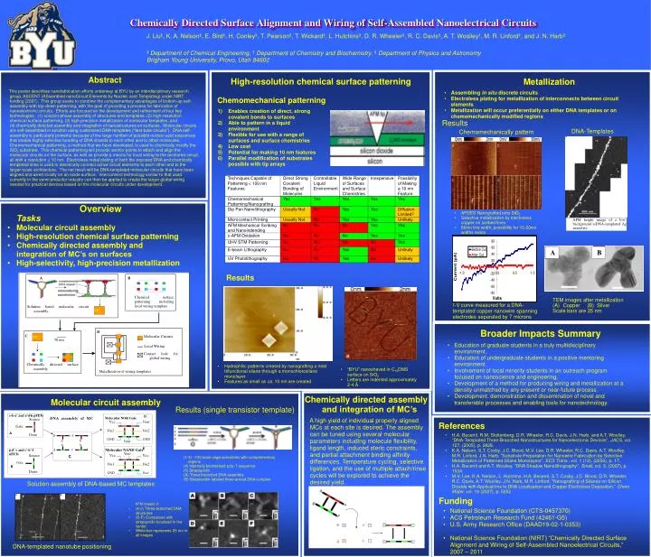
e-b-a' and a-d-h pFETs. Source. Gate. a. a'. Drain. h. e. d. b. Chemical surface patterning including local wiring template. d '. b '. Molecular NAND Gate. g. f. c. c'. Vout. Source. Vcc. Vcc. Gate. Vin1. Vin2. Drain. GND. Vout. B. A. A. B. 250 nm. 1000 nm.

E N D
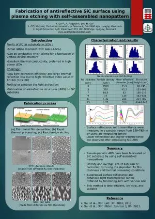
e-b-a' and a-d-h pFETs Source Gate a a' Drain h e d b Chemical surface patterning including local wiring template d' b' Molecular NAND Gate g f c c' Vout Source Vcc Vcc Gate Vin1 Vin2 Drain GND Vout B A A B 250 nm 1000 nm A B AFM height image of a low- background ssDNA‑templated Ag nanowire D DNA assembly of MC Molecular NOR Gate Vcc Vout Vin1 Vin2 A Solution based molecular circuit assembly h' e' MC GND GND Vout g' f ' E g-d'-c and c'-b'-f nFETs C D C Molecular Circuits MC B 50 nm Local Wiring Contact hole for global wiring Chemically directed surface assembly Metallization of wiring templates J. Liu‡, K. A. Nelson‡, E. Bird‡, H. Conley§, T. Pearson§, T. Wickard†,L. Hutchins‡, D. R. Wheeler‡, R. C. Davis§, A. T. Woolley†, M. R. Linford†, and J. N. Harb‡ ‡Department of Chemical Engineering, †Department of Chemistry and Biochemistry, §Department of Physics and Astronomy Brigham Young University, Provo, Utah 84602 Chemically Directed Surface Alignment and Wiring of Self-Assembled Nanoelectrical Circuits Abstract High-resolution chemical surface patterning Metallization This poster describes nanofabrication efforts underway at BYU by an interdisciplinary research group, ASCENT (ASsembled nanoCircuit Elements by Nucleic acid Templating) under NIRT funding (2007). This group seeks to combine the complementary advantages of bottom-up self-assembly with top-down patterning, with the goal of providing a process for fabrication of nanoelectronic circuits. Efforts are focused on the development and refinement of four key technologies: (1) solution-phase assembly of structures and templates, (2) high-resolution chemical surface patterning, (3) high-precision metallization of molecular templates, and (4) chemically directed assembly and integration of nanostructures on surfaces. Molecular circuits are self-assembled in solution using customized DNA templates (“test-tube circuits”). DNA self-assembly is particularly powerful because of the large number of possible nucleic-acid sequences that enable highly selective bonding of DNA strands to each other and to other molecules. Chemomechanical patterning, a method that we have developed, is used to chemically modify the SiO2 substrate. This chemical patterning will provide anchor points to attach and align the molecular circuits on the surface, as well as provide a means for local wiring to the anchored circuit, all with a resolution < 10 nm. Electroless metal plating of both the exposed DNA and chemically templated lines is used to electrically connect active circuit elements to each other and to the larger-scale architecture. The net result will be DNA-templated molecular circuits that have been aligned and wired locally on an oxide surface. Interconnect technology similar to that used currently in the semiconductor industry can then be applied to create the larger global wiring needed for practical devices based on the molecular circuits under development. • Assembling in situ discrete circuits • Electroless plating for metallization of interconnects between circuit elements • Metallization will occur preferentially on either DNA templates or on chemomechanically modified regions Chemomechanical patterning • Enables creation of direct, strong covalent bonds to surfaces • Able to pattern in a liquid environment • Flexible for use with a range of surfaces and surface chemistries • Low cost • Potential for making 10 nm features • Parallel modification of substrates possible with tip arrays Results DNA-Templates Chemomechanically pattern Overview • APDES Nanografted onto SiO2 • Selective metallization by electroless copper on scribed lines • 80nm line width, possibility for 10-20nm widths exists • Tasks • Molecular circuit assembly • High-resolution chemical surface patterning • Chemically directed assembly and integration of MC’s on surfaces • High-selectivity, high-precision metallization A B Results • TEM images after metallization • Copper (B) Silver • Scale bars are 25 nm I-V curve measured for a DNA-templated copper nanowire spanning electrodes separated by 7 microns Broader Impacts Summary • Education of graduate students in a truly multidisciplinary environment. • Education of undergraduate students in a positive mentoring environment. • Involvement of local minority students in an outreach program focused on nanoscience and engineering. • Development of a method for producing wiring and metallization at a density unmatched by any present or near-future process. • Development, demonstration and dissemination of novel and transferable processes and enabling tools for nanotechnology. • Hydrophilic patterns created by nanografting a neat trifunctional silane through a monochlorosilane monolayer • Features as small as ca. 10 nm are created • “BYU” nanoshaved in C18DMS surface on SiO2 • Letters are indented approximately 2-4 Å Chemically directed assembly and integration of MC’s Molecular circuit assembly Results (single transistor template) A high yield of individual properly aligned MCs at each site is desired. The assembly can be tuned using several molecular parameters including molecule flexibility, ligand length, induced steric constraints, and partial attachment binding affinity differences. Temperature cycling, selective ligation, and the use of multiple attach/rinse cycles will be explored to achieve the desired yield. References • H.A. Becerril, R.M. Stoltenberg, D.R. Wheeler, R.C. Davis, J.N. Harb, and A.T. Woolley, "DNA-Templated Three-Branched Nanostructures for Nanoelectronic Devices", JACS, vol. 127, (2005), p. 2828. • K.A. Nelson, S.T. Cosby, J.C. Blood, M.V. Lee, D.R. Wheeler, R.C. Davis, A.T. Woolley, M.R. Linford, J.N. Harb, "Substrate Preparation for Nanowire Fabrication by Selective Metallization of Patterned Silane Monolayers", ECS Trans., vol. 1 (12), (2006), p. 17. • H.A. Becerril and A.T. Woolley, "DNA Shadow Nanolithography", Small, vol. 3, (2007), p. 1534. • M.V. Lee, K.A. Nelson, L. Hutchins, H.A. Becerril, S.T. Cosby, J.C. Blood, D.R. Wheeler, R.C. Davis, A.T. Woolley, J.N. Harb, M.R. Linford, "Nanografting of Silanes on Silicon Dioxide with Applications to DNA Localization and Copper Electroless Deposition," Chem. Mater. vol. 19 (2007), p. 5052 (1-3) ~120 base oligonucleotides with complementary regions (4) Internally biotinylated poly-T sequence (5) Streptavidin (A) Three-branched DNA assembly (B) Streptavidin-labeled three-armed DNA complex Solution assembly of DNA-based MC templates Funding • AFM images of • (A-C) Three-branched DNA structures • (D-F) Complexes with streptavidin localized in the center • White bar represents 25 nm in all images • National Science Foundation (CTS-0457370) • ACS Petroleum Research Fund (42461-G5) • U.S. Army Research Office (DAAD19-02-1-0353) • National Science Foundation (NIRT) “Chemically Directed Surface Alignment and Wiring of Self-Assembled Nanoelectrical Circuits,” 2007 – 2011 DNA-templated nanotube positioning