Download
1 / 17
170 likes | 430 Views
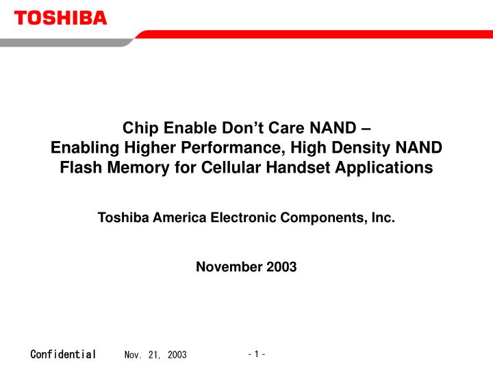
Chip Enable Don’t Care NAND – Enabling Higher Performance, High Density NAND Flash Memory for Cellular Handset Applications. Toshiba America Electronic Components, Inc. November 2003. Modified NAND Flash for easier integration in cell phones or other CE devices with complex memory subsystems.

E N D
Chip Enable Don’t Care NAND – Enabling Higher Performance, High Density NAND Flash Memory for Cellular Handset Applications Toshiba America Electronic Components, Inc. November 2003
Modified NAND Flash for easier integration in cell phones or other CE devices with complex memory subsystems. Targeted to address growing file storage requirements in cell phones Conventional NAND flash requires that the chip enable signal line be asserted low during the entire read cycle which prevents the processor from communicating with other devices on the same bus Chip Enable “Don’t Care” NAND flash allows the microprocessor to communicate with other devices on the bus such as SRAM, PSRAM or NOR flash while the NAND retrieves the information requested. Enables easier integration of NAND with NOR, SRAM and PSRAM in a system Initially available in 128Mb (TC581282AXB) and 256Mb (TC582562AXB) densities (.16 micron). New part numbers after die shrink to 0.13 micron in Q3 2003 are TC58DDM82A1 (256Mb, 1.8V core and I/O) and TC58DDM82A1 (256Mb, dual power 2.5V to 3.6V for VCC and 1.65V to 1.85V for VCCQ). CEDC feature also now available in large block NAND in densities of 1Gb and 2Gb Chip Enabled “Don’t Care” NAND
Conventional “Talk-only” Cell phones used NOR + SRAM for code storage, backup and data storage memory requirements As cell phone applications have increased, the need for increased data storage for music, photo and data storage, as well as additional software application storage has made NAND Flash more attractive because of its faster program and erase times, higher density and smaller cell size. Chip Enable Don’t Care NAND makes NAND flash much easier to combine with NOR and other types of memory in memory subsystems (or multi-chip packages) with multiple types of memory CEDC NAND can be used in conventional cell phone architectures which combine NOR+SRAM+NAND or in newer NAND + low power SDRAM architectures. NOR+SRAM+NAND MCP solutions are rapidly gaining in acceptance among cell phone manufacturers MCP Memory Subsystem Trend
M 527 Select pageN Cell array Figure 3. Read mode (1) operation A (00H)0 527 Sequential Read (1) NAND Flash Read Function Options Type-1(TSOP Package) Sequential Read /CE /WE /RE R/B Busy Data Output N M I/O 00H Sequential Read Start-address input Type-2 (BGA/MCP Package) Chip Enable Don’t Care No Sequential Read /CE don’t care /CE /WE /RE R/B Busy Data Output N M I/O 00H Start-address input Next Add. Input
Memory Requirements for Cellular Phones Large Density High Speed Low Cost Low Power 64M-128M RAM Movie / Music Buffer Working Area PSRAM LP SDRAM 16M-32M Data Backup 8M-16M 8M-16M Low Power 8M-16M LP-SRAM 4M-8M MCP Talk only Browse phone 3G High Speed 16M 32M-64M 64M-128M 128M-256M Boot & Basic Program NOR 128M-512M Large Density Low Cost High Speed program Flash Movie / Music App. Soft Storage NAND
Application Trend and Onboard Memory Size Memory size is increased bydiversity of application .
Multi-Chip Package for Mobile Phone Demand from Mobile Phone Market MCP Solution Low cost solution Embedded High-Density NAND (128M/256M/512M +) High-Density Pseudo SRAM (32M/64M/128M) Demand of large density RAM and Flash. Increase of various application High-speed requirement for execution of application software (PSRAM/NOR) + High-Speed Function(PSRAM/NOR) 8Page Mode: 25ns→18ns Burst Mode 15ns Multi-chip packages combine a complete, complex memory subsystem in a single, small component
Architectures for next generation phones • Conventional solution • Code : NOR • Work : Pseudo-SRAM • Data : NAND • Backup : SRAM (in Japanese market) with burst mode • Cost oriented solution • Code & Data : NAND • Work : LP-SDRAM with shadowing architecture
Mobile MCP Memory Trend End 2005 > 90% Camera Phones MP/Y 2001 < 10% Camera Phones SDRAM+NAND Production volume NAND+NOR+RAM NOR+RAM CY From 2003, NAND becoming popular in Europe and US (already popular in Asia) driven by storage requirements Source: Toshiba Internal Data/Projections
1.6 1.6 9x12 9x12 1.4 1.4 9x12 1.4 7x10 1.2 Trend of Multi-Chip Package more 7Chip over 5/6Chip St-MCP 9x12 3/4Chip St-MCP (NOR+NOR+SRAM+PSRAM) Stacked MCP 9x12 1.4 9 x 12 (SRAM+NOR) (NAND+NOR+PSRAM) (4MS+32MF) 3Chip Package Area 9x12 0.8mm pitch (16MS+64MF) Small 69 balls(Actual 56balls) 1.2 9x12 1.2 7x10 4Chip 1.4 7x10 3Chip 1.2 Small form factor 7 x 10 (8/4MS+64/32MF) 2000 2001 2002 2003 2004 CY
Chip5 Chip4 Chip3 Chip2 Chip1 Chip2 Chip3 Chip1 Chip5 Chip4 5-chip Stacked-MCP Technology TOSHIBA 5Chip St-MCP 1.6mm Max WIRE BOND PKG SIZE 9x12 7x10
NOR NAND ~ 128Mbit ~ 1Gbit 3V, 1.8V 3V, 1.8V x8/x16 x8/x16 50ns(serial access cycle) 25ms(random access) 70ns(30pF, 2.3V) 65ns(30pF, 2.7V) 8ms/Byte 4.1ms/512Byte 200ms/512Byte 2ms/Block (16KB) 700ms/Block 1.23s/Block (main:64KB) 33.6ms / 64KB (x8) NAND / NOR Characteristics Capacity Power Supply I/O Access Time Program Speed (typ.) Erase Speed(typ.) Prog+Erase(typ.)
NAND Word line Unit Cell Source line 2F 2F 5F 2F 4F2 NAND vs. NOR - Cell Structure NOR Bit line Contact Word line Cell Array Unit Cell Source line Layout Cross- section Cell size 10F2
NAND2LC 1.5ms NAND4LC Slow 2ms NOR 2LC 2s NOR 4LC 1.2s Performance comparison Read Program NAND2LC NAND2LC 8.3MB/s 27MB/s NAND4LC Fast NAND4LC 20.5MB/s 1.7MB/s Fast 55.2MB/s NOR 2LC NOR 2LC 0.15MB/s 0.145MB/s NOR 4LC NOR 4LC 50.0MB/s Erase
Performance comparison NAND 2LC NAND 4LC NOR 2LC NOR 4LC 55.2MB/s 50.MB/s 27MB/s 20.5MB/s Read 80ns+30nsx7 for 16 bytes 25us+50nsx1056 for 2k bytes 50us+50nsx1056 for 2k bytes 85ns+25nsx3 for 8 bytes 0.15MB/s 0.145MB/s 8.3MB/s 1.7MB/s Prog. 107µs for 16 bytes 440µs for 64 bytes 50nsx1056+200µs for 2k bytes 50nsx1056+1.2ms for 2k bytes 2s 1.2s 2ms 1.5ms Erase 64 Kbytes 128 Kbytes 128 Kbytes 128 Kbytes
Memory requirements in high-end cell phones have increased dramatically to support new applications Different types of memory are best suited for different applications Code storage Working memory File and additional application storage Multi-chip packages (MCP) enable complex memory subsystems in a single component Traditional NOR +SRAM memory solutions for cell phones are being replaced by NOR+PSRAM+NAND and other combinations of multiple memories One newer low-cost alternative is NAND + Low Power SDRAM Chip Enable Don’t Care NAND Flash makes integration of NAND with other memory types much easier. Summary
Information in this presentation, including product pricing and specifications, and content of services is current on the date issued, but is subject to change without prior notice. All trademarks and tradenames held within are the properties of their respective holders.