Download
1 / 54
550 likes | 697 Views
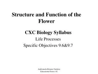
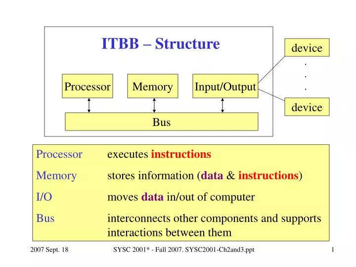
device. ITBB – Structure. Processor. Memory. Input/Output. device. Bus. Processor executes instructions Memory stores information ( data & instructions ) I/O moves data in/out of computer Bus interconnects other components and supports interactions between them.

E N D
device ITBB – Structure . . . Processor Memory Input/Output device Bus Processor executes instructions Memory stores information (data & instructions) I/O moves data in/out of computer Bus interconnects other components and supports interactions between them SYSC 2001* - Fall 2007. SYSC2001-Ch2and3.ppt
ITBB: Fundamental Binary Assumption • all information is binary encoded • result of transistor technology • one bit = one binary digit value either 0 or 1 • one Byte = 8 bits grouped together b7b6b5b4b3b2b1b0 e.g. 100111012 vs. 1001110110 • one word = machine dependent number of bits • information includes dataand instructions! case! msb lsb indicates base of number SYSC 2001* - Fall 2007. SYSC2001-Ch2and3.ppt
Encoding (Representing) Data Using Binary Values • counting numbers see Assignment 1 • integers (format defacto standard) • floating point (IEEE standard) • characters (ASCII, Unicode) • boolean • days of the week • colours • other ??? later – Ch. 9 later – assembly language application / implementation dependent ( SYSC 2003 ) SYSC 2001* - Fall 2007. SYSC2001-Ch2and3.ppt
Encoding (Representing) Instructions Using Binary Values • use some bits to encode operation opcode • use some bits to encode operands (if present) • for now, assume fixed number of bits ( w ) per instruction • fixed number of bits ( i ) used for opcode • fixed number of bits ( j ) used for operand(s) w bits opcode operands i bits j bits SYSC 2001* - Fall 2007. SYSC2001-Ch2and3.ppt
ITBB Function Function lecture 2 • Recall functions in a computer: • Data PROCESSING • Data STORAGE • Data MOVEMENT • CONTROL • now we consider each component in terms of these functions and the roles of the components in the structure SYSC 2001* - Fall 2007. SYSC2001-Ch2and3.ppt
Processor ( a.k.a. CPU) CPU = Central Processing Unit • PROCESSINGarithmetic and logic unit ( ALU ) • manipulates/changes/combines/calculates data values • STORAGEregisters hold values in CPU • each register has a unique name • CONTROLcontrol unit • built-in instruction cycle engine that drives machine • instruction cycle drives control to memory and I/O components when appropriate ! SYSC 2001* - Fall 2007. SYSC2001-Ch2and3.ppt
Processor Structure • MOVEMENT • internal connections (control unit, ALU and registers) • external Bus connections to other components CPU ALU Registers Control Unit external Bus connections internal connections SYSC 2001* - Fall 2007. SYSC2001-Ch2and3.ppt
Processor Instruction Cycle START cycle fetch instruction ( from memory ) execute the instruction may cause more memory accesses (for operands) HALT SYSC 2001* - Fall 2007. SYSC2001-Ch2and3.ppt
IMPORTANT SLIDE ! Memory ( 1 ) • STORAGE • fixed width locations (or cells) • each location contains information • contents: the value stored in the location • address: unique “name” for each location • MOVEMENT • internal connections • external bus connections e.g. house numbers memory does not differentiate contents as instructions vs. data ( its all just binary values ) SYSC 2001* - Fall 2007. SYSC2001-Ch2and3.ppt
Memory ( 2 ) • PROCESSING (limited processing compared to CPU) • refresh? transistor technology • bit-level error checking? error correction ? • CONTROL (of memory actions) • write – copy input value as new contents of a location • read – output (but do not modify) contents of a location • write / read driven from “outside” (e.g. processor, other ?) • may provide external control error condition? Ch. 5 later SYSC 2001* - Fall 2007. SYSC2001-Ch2and3.ppt
Memory Structure Memory memory processor locations Control Unit external Bus connections internal connections SYSC 2001* - Fall 2007. SYSC2001-Ch2and3.ppt
Input Output ( 1 ) • function depends on connected devices • STORAGE fixed width registers (or ports) • each register contains information • contents: the value stored in the register • address: unique “name” for each register • MOVEMENT • internal connections • external bus connections SYSC 2001* - Fall 2007. SYSC2001-Ch2and3.ppt
Input Output ( 2 ) Ch. 7 • PROCESSING • device dependent ! specialized hardware • CONTROL (of device-related processing) • write – copy input value as new contents of a port • read – output contents of a port • not always the case that can read & write a port ! • write / read driven from “outside” (e.g. processor, other) • may drive external control interrupts ! SYSC 2001* - Fall 2007. SYSC2001-Ch2and3.ppt
Input Output Structure N. B. I/O component = Memory ! device I/O device processor registers ( ports ) Control Unit external Bus connections internal connections SYSC 2001* - Fall 2007. SYSC2001-Ch2and3.ppt
Bus • pathway for interactions among components • standard signaling protocols for using the Bus • specified using timing diagrams • MOVEMENTYES! • CONTROL arbitration (traffic cop) • resolve concurrent requests to use the Bus • STORAGE not usually • PROCESSING not usually Appendix 3A sometimes … arbiter SYSC 2001* - Fall 2007. SYSC2001-Ch2and3.ppt
Putting ITBB Together - A “Simplified IAS-like” Example ( sIAS ) • Want an example to show simple instruction execution • need details for: • sIAS memory: locations • sIAS processor: instructions, registers, instruction cycle • further simplification: assume decimal (instead of binary or hexadecimal) values • this example ignores: bus protocols, I/O, control details See IAS Ch. 2.1, IAS-like, “Hypothetical” Ch 3.1, 3.2 SYSC 2001* - Fall 2007. SYSC2001-Ch2and3.ppt
sIAS Memory Memory address contents 000 1234 001 9075 002 6386 . . . . . . 997 3180 998 6724 999 9932 location • contents: store 4-digit decimal values • address: a 3-digit decimal value • since each address is unique total address space = 1000 largest possible number of locations SYSC 2001* - Fall 2007. SYSC2001-Ch2and3.ppt
sIAS Processor – Registers CPU Registers ALL reg’s hold 4 digit decimal values PC: address of next instruction to fetch IR: holding register for instruction after fetch AC: data register “accumulator” MAR: memory address register MBR: memory buffer register 825 PC 2001 IR 0000 AC MAR 0024 MBR 2001 SYSC 2001* - Fall 2007. SYSC2001-Ch2and3.ppt
sIAS Instruction Cycle means “gets loaded with” 1. Fetch Instruction • MAR PC // set up address for fetch • MBR Mem[ MAR ] // fetch instruction • IR MBR // save instruction • PC PC + 1 // set up for next fetch 2. Execute instruction in IR may involve memory access built-in sequential execution of instructions!! SYSC 2001* - Fall 2007. SYSC2001-Ch2and3.ppt
sIAS Processor – Instructions 4-digit Encodings Operation 1xxx Load AC value from memory address xxx 2xxx Store AC value to memory address xxx 3xxx Add contents of memory address xxx to AC = opcode encoding = operand encoding • Example instructions: 1376 2378 3379 • if executed, what effect would these have on the CPU and memory? SYSC 2001* - Fall 2007. SYSC2001-Ch2and3.ppt
Consider Example sIAS State CPU Registers Memory address contents 224 1826 225 1827 226 3828 227 2828 826 9999 827 0001 828 0009 829 0000 0225 PC . . . . . . 1826 IR 9999 AC . . . . . . MAR 0826 MBR 2001 . . . . . . SYSC 2001* - Fall 2007. SYSC2001-Ch2and3.ppt
1st Instruction Cycle Iteration – Fetch • Fetch a) MAR 0225 PC b) MBR 1827 Mem[ 0225 ] c) IR 1827 MBR d) PC 0226 PC + 1 instruction fetched: 1827 Load AC value from memory address 827 SYSC 2001* - Fall 2007. SYSC2001-Ch2and3.ppt
1st Instruction Cycle Iteration – Execute • execute instruction in IR: 1827 • Load AC value from memory address 827 a) MAR 0827 from IR b) MBR 0001 Mem[ 827 ] c) AC 0001 from MBR SYSC 2001* - Fall 2007. SYSC2001-Ch2and3.ppt
2nd Instruction Cycle Iteration – Fetch Memory address contents 224 1826 225 1827 226 3828 227 2828 826 9999 827 0001 828 0009 829 0000 • Fetch a) MAR 0226 PC b) MBR 3828 Mem[0226] c) IR 3828 MBR d) PC 0227 PC + 1 instruction fetched: 3828 Add contents from memory address 828 to AC SYSC 2001* - Fall 2007. SYSC2001-Ch2and3.ppt
2nd Instruction Cycle Iteration – Execute • execute instruction in IR: 3828 • Add value from memory address 828 to AC a) MAR 0828 from IR b) MBR 0009 Mem[ 828 ] c) AC 0010 AC + MBR SYSC 2001* - Fall 2007. SYSC2001-Ch2and3.ppt
3rd Instruction Cycle Iteration – Fetch • Fetch a) MAR 0227 PC b) MBR 2828 Mem[ 0227 ] c) IR 2828 MBR d) PC 0228 PC + 1 instruction fetched: 2828 Store AC value to memory address 828 SYSC 2001* - Fall 2007. SYSC2001-Ch2and3.ppt
3rd Instruction Cycle Iteration – Execute • execute instruction in IR: 2828 • Store AC value into location at address 828 a) MAR 0828 from IR b) MBR 0010 AC c) Mem[ 828 ] 0010 MBR SYSC 2001* - Fall 2007. SYSC2001-Ch2and3.ppt
Instruction Cycle - State Diagram access to memory no operands SYSC 2001* - Fall 2007. SYSC2001-Ch2and3.ppt
Interrupts • Mechanism to interrupt normal sequence of processing • Why? • I/O events: e.g. mouse click, network data arrives • timer: e.g. animation • program exception: e.g. overflow, division by zero • hardware error: e.g. memory error • these are asynchronous events! require programmed service • events caused by hardware, not software instructions Ch. 7.4 Unpredictable timing SYSC 2001* - Fall 2007. SYSC2001-Ch2and3.ppt
interrupt handler (a.k.a. ISR) “driver”? An Interrupt Scenario independent execution contexts “threads of control” App. code eg. audio CD Suppose App. code executing: • interrupt occurs • want ISR to run • then resume App. ISR = Interrupt Service Routine performs s/w action appropriate to interrupt event eg. editor want to share processor between threads! SYSC 2001* - Fall 2007. SYSC2001-Ch2and3.ppt
interrupt handler Transfer of Control via Interrupts App. code 5 2 interrupt occurs during execution of instruction at i 1 3 suspend thread ! hardware invokes interrupt handler resume thread @ i+1 6 4 SYSC 2001* - Fall 2007. SYSC2001-Ch2and3.ppt
Extending Instruction Cycle for Interrupts • after instruction execute phase of cycle – processor checks: • exception occurred? e.g. divide by 0 • interrupt event signal input to processor? • If interrupt pending: • Suspend and save context of current thread of execution • Set PC to start address of ISR • Continue Cycle fetch 1st instruction of ISR code • Eventually, ISR s/w restores context resume interrupted thread • If no interrupt pending: Continue Cycle fetch next instruction done by processor h/w – no s/w ! SYSC 2001* - Fall 2007. SYSC2001-Ch2and3.ppt
hmmmm….. last 3 slides all say the same thing Extending Processor Instruction Cycle START cycle no interrupt pending save context & set PC to start address of interrupt handler fetch instruction execute instruction yes HALT SYSC 2001* - Fall 2007. SYSC2001-Ch2and3.ppt
Signals: “here is the data”, “read the contents of this address”, “I want to use the bus”, etc. Digital Signaling • signals are indicated as voltage levels • use particular levels to represent binary values • e.g. +5 volts 1 0 volts 0 • change values “quickly” Or could be –5V, 0V or…? want to avoid reading when not stable signals stable 1 0 time SYSC 2001* - Fall 2007. SYSC2001-Ch2and3.ppt
App. 3A Signals and Timing Diagrams rising (leading) edge falling (trailing) edge ~ ~ • often bundle groups of related signals as one in a timing diagram e.g. 16-bit addresses 16 address signals one per bit 1 0 indefinite time elapsed signals stable, represent a useful 16-bit address signals may be stable, but do not represent a useful value 1 address 0 SYSC 2001* - Fall 2007. SYSC2001-Ch2and3.ppt
Bus • communication pathway connecting components • shared communications broadcast to all on bus • organize communicated information into 3 groups: • address • data • control of information being communicated everything else SYSC 2001* - Fall 2007. SYSC2001-Ch2and3.ppt
Bus Interconnection Scheme I/O memory SYSC 2001* - Fall 2007. SYSC2001-Ch2and3.ppt
Data Bus • carries data • remember that there is no difference between “data” and “instruction” at this level • data bus width is a key determinant of performance • 8, 16, 32, 64 bit SYSC 2001* - Fall 2007. SYSC2001-Ch2and3.ppt
Address bus • identify the source or destination of data • e.g. CPU needs to read an instruction (data) from a given location in memory • address bus width determines maximum memory capacity of system (address space) • e.g. 8080 has 16 bit address bus giving 64k address space 216 SYSC 2001* - Fall 2007. SYSC2001-Ch2and3.ppt
1 address 0 1 data 0 1 address data 0 Address and Data Groups • often bundle address and data signals separately and use different physical pathways • may multiplex using same physical pathway SYSC 2001* - Fall 2007. SYSC2001-Ch2and3.ppt
Some Common Control Signals • reset – force all components to reset • clock(s) to synchronize communication • destination indicator – usually memory or I/O • acknowledgment from component – info received • interrupts • arbitration “hand shake” SYSC 2001* - Fall 2007. SYSC2001-Ch2and3.ppt
Bus Protocols • signaling and sequencing to permit interactions between components • processor puts address value on bus, and “memory read” control indication • memory receives read signal, reads address, gets appropriate data, puts data on bus • processor waits, then reads data from bus • May be • Synchronous - synchronized by a clock – organize protocol by clock “ticks” Ti • Asynchronous – no pacing by a shared clock e.g. memory read SYSC 2001* - Fall 2007. SYSC2001-Ch2and3.ppt
E.G. Synchronous Memory Read T1 T2 T3 Assumption: Sensing of bus signals done during clock trailing edge clock mem read stable address addrs stable data data T1 initiate memory read (addrs, mem read) T2 time for memory to do internal work T3 data ready for reading from bus SYSC 2001* - Fall 2007. SYSC2001-Ch2and3.ppt
E.G. Asynchronous Memory Write no shared clock pacing the protocol mem write command processor memory SYSC 2001* - Fall 2007. SYSC2001-Ch2and3.ppt
Single Bus Problems • lots of devices on one bus leads to: • propagation delays • long data paths mean that co-ordination of bus use can adversely affect performance • if aggregate data transfer approaches bus capacity • most systems use multiple buses to overcome these problems evolution for performance! SYSC 2001* - Fall 2007. SYSC2001-Ch2and3.ppt
Traditional bus (with cache) Ch. 4 Processor Cache: Remembers data from previous requests. Can processor request be answered from cache? If not pass request on via system bus Memory aka Front side bus I/O SYSC 2001* - Fall 2007. SYSC2001-Ch2and3.ppt
High Performance Bus faster devices FireWire slower devices SYSC 2001* - Fall 2007. SYSC2001-Ch2and3.ppt
PCI Bus • Peripheral Component Interconnection Bus • Intel released to public domain • 32 or (optional) 64 bit address/data bus • 49 mandatory lines • Note: 64 data lines @ 66 Mhz = 528 MBps = 4.2 Gbps • synchronous • read bus on rising clock • modify bus on falling clock rules for use ! SYSC 2001* - Fall 2007. SYSC2001-Ch2and3.ppt
PCI Bus Lines (required) • System lines • including clock and reset • Address & Data (AD) • 32 lines each: multiplexed • interrupt & validate lines • Interface Control • C / BE – command / byte enable: multiplexed • Arbitration • Error lines text: table 3.3 more optional lines too! SYSC 2001* - Fall 2007. SYSC2001-Ch2and3.ppt
PCI Commands • overview of a transaction between initiator (master) and target, e.g. CPU initiates a read from memory • master claims bus arbitration & wait for idle • specify type of transaction e.g. I/O read/write • address phase ( address & command ) • one or more data phases ( data & byte enable) SYSC 2001* - Fall 2007. SYSC2001-Ch2and3.ppt