Download

1 / 4
100 likes | 265 Views
PCB manufacturing. PCBpro.com. Step#1 Film Generation: Generated from your design files, we create an exact film representation of your design. We will create one film per layer. Step#2 Shear Raw Material:

E N D
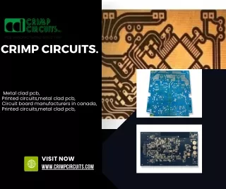
PCB manufacturing PCBpro.com
Step#1 Film Generation: Generated from your design files, we create an exact film representation of your design. We will create one film per layer. Step#2 Shear Raw Material: Industry standard 0.059" thick, copper clad, two sides. Panels will be sheared to accommodate many boards. Step#3 Drill Holes: Using NC machines and carbide drills. Step#4 Electroless Copper: Apply thin copper deposit in hole barrels.
Step#5 Apply Image: Apply photosensitive dryfilm (plate resist) to panel. Use light source and film to expose panel. Develop selected areas from panel. Step#6 Pattern Plate: Electrochemical process to build copper in the holes and on the trace area. Apply tin to surface. Step#7 Strip & Etch: Remove dryfilm, then etch exposed copper. The tin protects the copper circuitry from being etched. Step#8 Solder mask: Apply solder mask area to entire board with the exception of solder pads.
Step#9 Solder coat: Apply solder to pads by immersing into tank of solder. Hot air knives level the solder when removed from the tank. Step#10 Nomenclature: Apply white letter marking using screen printing processStep#11 Fabrication: Route the perimeter of the board using NC equipment