Download
1 / 25
640 likes | 2.12k Views
Stress control of thin films in Plasma deposition. By: Liwei Wang Professor: Dr. Y. Tzeng For: ELEC 7730 Date: Nov 10, 2003. Questions. What is the microstructure formed during film growth cause the intrinsic tensile stress?

E N D
Stress control of thin films in Plasma deposition By: Liwei Wang Professor: Dr. Y. Tzeng For: ELEC 7730 Date: Nov 10, 2003
Questions • What is the microstructure formed during film growth cause the intrinsic tensile stress? • How is dual frequency in PECVD control the stress of thin films?
Outline • Background Introduction • ---Why it is important to control the stress in the • thin films deposition? • ---Where is the stress in the thin films come from? • Thin film deposition techniques • ---How to control the stress of Plasma deposited • thin films? • Case study
Why do we need to study the stress in thin films? • To control: • High stress in thin films can cause • --- Adhesion problems. • --- Long-term reliability. • To make use of: ---Use of the connection between stress and structure for producing nanostructure.
Causes of Stress in the Thin film • Extrinsic: • – A non-uniform plastic deformation. • – Thermal stress • Intrinsic: • – Growth stresses • – Lattice misfit • – Substitutional or interstitial impurities • – Volume changes by phase transformation
Extrinsic stress--Thermal Stress Thermal Stress results from the difference in the thermal expansion coefficients of the substrate and the film. http://mmadou.eng.uci.edu/Classes/MSE621/MSE62101(14).pdf.
Intrinsic stress– Growth stresses • Intrinsic stress results from the microstructure created in the film as atoms are deposited on the substrate. • At substrate temperatures less than 20% of the melting point, intrinsic stress due to incomplete structural ordering dominates.
Classification of stresses in thin films • Biaxial stresses • – Compressive. • – Tensile. • Shear and normal stresses: • – Only important near edge. • – Important for fine line pattern in Microelectronic.
Biaxial stresses Compressive stress Tensile stress The film wants to be "smaller" than the substrate because it was "stretched" to fit. The film wants to be "larger" than the substrate, because it was "compressed" to fit. Stress Control in NiV, Cr and TiW Thin Films used in UBM and Backside Metallization, K. O’Donnell, J. Kostetsky, and R.S. Post
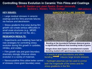
Tensile stress Microvoids formed during film growth cause attractive interaction of atoms across the voids. Y. Fu et al. / Surface and Coatings Technology 167 (2003) 120–128
Compressive stress • Impact of heavy ions or energetic particles during deposition (like hitting film with a hammer), can pack atoms more tightly. Compressive stress. • Atomic Peening - Energetic Particle Bombardment of growing film at low sputter pressures results in a dense film with compressive stress.
Stress control in Sputtering deposition Working gas Process parameters such as: Sputtering pressure Negative Bias voltage. http://www.postech.ac.kr/mse/tfxs/2003_2/chapter3.pdf
Sputtering pressure control Sputtering Film: --TiW (high mass) --3000A Figure. Stress control in TiW film by varying sputtering pressures Stress Control in NiV, Cr and TiW Thin Films used in UBM and Backside Metallization, K. O’Donnell, J. Kostetsky, and R.S. Post
Sputtering pressure control Figure. AFM Imaging of TiW films processed at 2, 11, and 20 mtorr. Stress Control in NiV, Cr and TiW Thin Films used in UBM and Backside Metallization, K. O’Donnell, J. Kostetsky, and R.S. Post
Sputtering pressure control • The surface morphology indicate: -A dense microstructure in the TiW sputter deposited at 2 mTorr which is reflected in the large compressive stress measured for this film (- 1800 MPa). -A dense to a voided microstructure change in the TiW film deposited at 20 mTorr which is reflected in the tensile stress measured for this film (+700 MPa). • The increase in resistivity is consistent with the development of such a voided structure.
Stress control with RF bias voltage Sputtering Film: --NiV (low mass) --Cr (low mass) --4000A Figure. Stress control in NiV and Cr films by varying RF bias voltage. Stress Control in NiV, Cr and TiW Thin Films used in UBM and Backside Metallization, K. O’Donnell, J. Kostetsky, and R.S. Post
Stress control in PECVD system http://tftlcd.kyunghee.ac.kr/research/poly-Si/chapter4.html
Stress control in PECVD system • Two main methods to control film stress in PECVD • Dual frequency PECVD • ---13.56MHz (HF) HF component used to control • electron density. • ---100-400kHz (LF) LF component used to control • plasma sheath voltage & ion energy • distribution • Gas flow
Dual frequency PECVD In a conventional reactor, increase the RF power to get a higher ion bombardment energy, the plasma density will also increase. • Two separate power supplies • Each attached to one electrode • Independent control of ion bombardment energy and plasma density. http://www.batnet.com/enigmatics/semiconductor_processing/CVD_Fundamentals/plasmas/Cap_parameters.html
Dual frequency control thin film stress • Films studied: • silicon nitride • silicon dioxide • Frequency interlacing 130 KHz (LF) • 13,56 MHz (HF) • Stress control • tensile 40 MPa compressive120 MPa http://www.oxfordplasma.de/process/sinsioka.htm
Stress control by gas flow in PECVD • Gas flow ratio • Neutral gas species
Gas flow ratio control film stress • Film deposited: • Hydrogenated amorphous silicon nitride (a-SiNx:H) • Gas Species: • SiH4-NH3-H2 Stress control of hydrogenated amorphous silicon nitride films deposited by PECVD, Hidenori Gamo1, Hideyuki Eguchi1, Toshiaki Kurosu1,Kiyoharu Nakagawa2,4, Mikka Nishitani-Gamo3, and Toshihiro Ando4
Neutral gas species control thin film stress • Film studied: • Hydrogenated amorphous silicon nitride (a-SiNx:H) • Gas Species: • SiH4-NH3-N2 • Stress control: • Through dilution of the film precursors with an inert gas. • Result: • The tensile stress in films without dilution reduces when argon • is added to the plasma due to the Si-H plasma chemistry and • film hydrogen bond density change. Chemical influence of inert gas on the thin film stress in plasma-enhanced chemical vapor deposited a-SiN :H films, M. J. Loboda and J. A. Seifferly
Conclusions • Stress control of Thin film attract wide attention because the huge influence to Microelectronic performance and applications. • Stress control can be achieved in sputtering by adjusting the sputtering pressure and negative bias voltage. • Stress control can be achieved in PECVD by employing dual frequency and changing gas flow.
Answers • What is the microstructure formed during film growth cause the intrinsic tensile stress? --- Microvoids formed during film growth cause attractive interaction of atoms across the voids. • How is dual frequency in PECVD control the stress of thin films? --- Independent control of ion bombardment energy and plasma density.