Download
1 / 8
180 likes | 667 Views
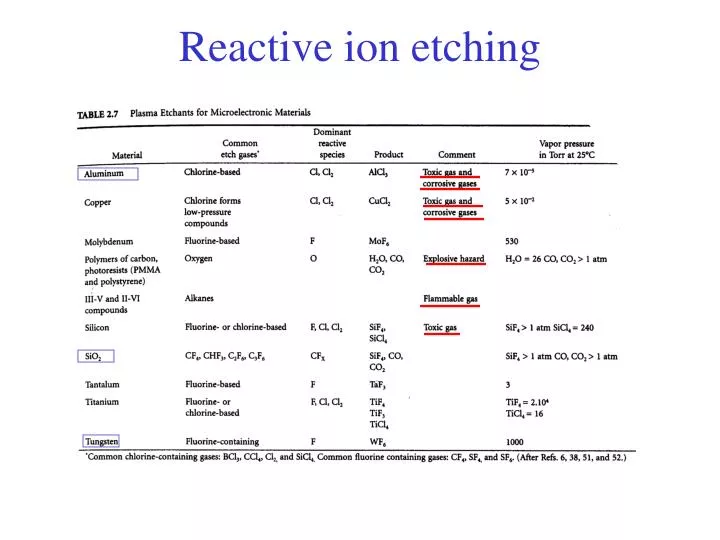
Reactive ion etching. Reactive ion etching. Material selectivity. Ion Beam milling @INESC. Nordiko 3000 IBD system. 65 W RF grids: +500V, -200V 8 sccm Ar 40% rotation 70º or 40º pan. Etch rates [Å/min] @ 70ºpan. 65 W 130 W * junctions, spin valves ~ 60

E N D
Reactive ion etching Material selectivity
Ion Beam milling @INESC Nordiko 3000 IBD system 65 W RF grids: +500V, -200V 8 sccm Ar 40% rotation 70º or 40º pan Etch rates [Å/min] @ 70ºpan 65 W 130 W * junctions, spin valves ~ 60 Al ~ 160 Al2O3 ~ 57 SiO2 ~ 170 CoZrNb ~ 130 Photoresist ~ 55 *PR baked @110ºC, 5 min.
Challenges in Dry etching Damage by surface charging Feature size control within a wafer Etch rate of a material depends on the surface area of the etchable material but a large unmasked area exposed to the beam consumes more etch species than a single trench – local modulation of the plasma chemistry. Etch rate of a material depends on the ratio feature size : feature depth Aspect ratio dependent etch rate
Etching end-point • Visual inspection • Direct measurements: sample electrical resistivity • Mass spectroscopy – monitor the chamber atmosphere composition during the etching
Patterning thick and hard materials Disk head slider machining – reactive ion etching SF6 etching TiC CF2 etching Al2O3 Temperature: 40-100ºC Etch ratio: Resist:AlTiC ~ 5:1 rate: 370-490 Å/min Surface smoothing: < 250Å Etch depth 0.5 to 5 mm Al2O3-TiC sliders
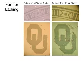
lead shield pm Ins. sv Ins. lead shield pm Patterning thin films to sub-micron Courtesy of Ed Murdoch, Seagate
Bibliography • VLSI Technology, S.M.Sze, McGraw-Hill International Editions • Nanoelectronics and information technology – Advanced Electronic Materials and • Novel Devices, Rainer Waser (Ed.), Wiley-VCH (2003) • Fundamentals of Microfabrication – The science of miniaturization, Marc J.Madou, CRC press (2002) • “Lift-off techniques for fine line metal patterning”, J.M.Frary and P.Seese, SEMICONDUCTOR INTERNATIONAL , pp.72-88 (December 1981) • “Ion etching for pattern delineation”, C.M.Melliar-Smith, J.Vac.Sci.Technol., Vol.13 (5), pp.1008-1022 (September 1976) • “Ion Beam Etching”, R.R.Puckett, S.L.Michel and W.E.Hughes, Thin Film Processes II, Chapt.V-2, Academic Press. Inc. (1991) • “Etch rates for Micromachining processing”, K.R.Williams and R.S.Muller, J.Microelectromechanical Systems, Vol.5 (4), pp.256-269 (December 1996) • “Reactive Ion etching of alumina/TiC substrates”, US Pattent nº 6,001,268 (IBM Corporation), 1997