Download
1 / 73
930 likes | 1.12k Views
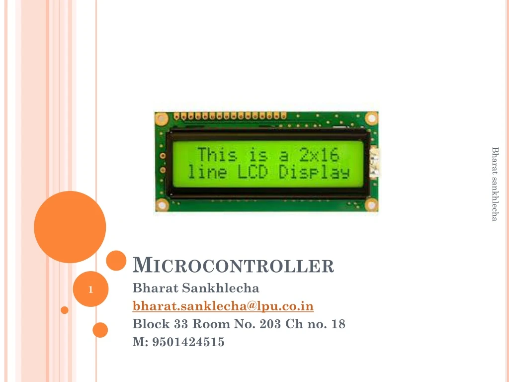
Microcontroller. Bharat Sankhlecha bharat.sanklecha@lpu.co.in Block 33 Room No. 203 Ch no. 18 M: 9501424515. LCD is finding widespread use replacing LEDs The declining prices of LCD The ability to display numbers, characters, and graphics

E N D
Microcontroller Bharat sankhlecha Bharat Sankhlecha bharat.sanklecha@lpu.co.in Block 33 Room No. 203 Ch no. 18 M: 9501424515
LCD is finding widespread use replacing LEDs • The declining prices of LCD • The ability to display numbers, characters, and graphics • Incorporation of a refreshing controller into the LCD, thereby relieving the CPU of the task of refreshing the LCD • Ease of programming for characters and graphics
ADCs (analog-to-digital converters) are among the most widely used devices for data acquisition • A physical quantity, like temperature, pressure, humidity, and velocity, etc., is converted to electrical (voltage, current) signals using a device called a transducer, or sensor • We need an analog-to-digital converter to translate the analog signals to digital numbers, so microcontroller can read them
ADC804 IC is an analog-to-digital converter • It works with +5 volts and has a resolution of 8 bits • Conversion time is another major factor in judging an ADC • Conversion time is defined as the time it takes the ADC to convert the analog input to a digital (binary) number • In ADC804 conversion time varies depending on the clocking signals applied to CLK R and CLK IN pins, but it cannot be faster than 110 μs
CLK IN and CLK R • CLK IN is an input pin connected to an external clock source • To use the internal clock generator (also called self-clocking), CLK IN and CLK R pins are connected to a capacitor and a resistor, and the clock frequency is determined by • Typical values are R = 10K ohms and C = 150 pF • We get f = 606 kHz and the conversion time is 110 μs
Vref/2 • It is used for the reference voltage • If this pin is open (not connected), the analog input voltage is in the range of 0 to 5 volts (the same as the Vcc pin) • If the analog input range needs to be 0 to 4 volts, Vref/2 is connected to 2 volts
D0-D7 • The digital data output pins • These are tri-state buffered • The converted data is accessed only when CS = 0 and RD is forced low • To calculate the output voltage, use the following formula
Analog ground and digital ground • Analog ground is connected to the ground of the analog Vin • Digital ground is connected to the ground of the Vcc pin • To isolate the analog Vin signal from transient voltages caused by digital switching of the output D0 – D7 • This contributes to the accuracy of the digital data output
The following steps must be followed for data conversion by the ADC804 chip • Make CS = 0 and send a low-to-high pulse to pin WR to start conversion • Keep monitoring the INTR pin • If INTR is low, the conversion is finished • If the INTR is high, keep polling until it goes low • After the INTR has become low, we make CS = 0 and send a high-to-low pulse to the RD pin to get the data out of the ADC804
Examine the ADC804 connection to the 8051 in Figure 12-7. Write a program to monitor the INTR pin and bring an analog input into register A. Then call a hex-to ACSII conversion and data display subroutines. Do this continuously.
A thermistor responds to temperature change by changing resistance, but its response is not linear • The complexity associated with writing software for such nonlinear devices has led many manufacturers to market the linear temperature sensor
The sensors of the LM34/LM35 series are precision integrated-circuit temperature sensors whose output voltage is linearly proportional to the Fahrenheit/Celsius temperature • The LM34/LM35 requires no external calibration since it is inherently calibrated • It outputs 10 mV for each degree of Fahrenheit/Celsius temperature
Signal conditioning is a widely used term in the world of data acquisition • It is the conversion of the signals (voltage, current, charge, capacitance, and resistance) produced by transducers to voltage, which is sent to the input of an A to- D converter • Signal conditioning can be a current-tovoltage conversion or a signal amplification • The thermistor changes resistance with temperature, while the change of resistance must be translated into voltage in order to be of any use to an ADC
Example: • Look at the case of connecting an LM35 to an ADC804. Since the ADC804 has 8-bit resolution with a maximum of 256 steps and the LM35 (or LM34) produces 10 mV for every degree of temperature change, we can condition Vin of the ADC804 to produce a Vout of 2560 mV full-scale output. Therefore, in order to produce the fullscale Vout of 2.56 V for the ADC804, We need to set Vref/2 = 1.28. This makes Vout of the ADC804 correspond directly to the temperature as monitored by the LM35.
KEYBOARD INTERFACING • Keyboards are organized in a matrix of rows and columns • The CPU accesses both rows and columns through ports • Therefore, with two 8-bit ports, an 8 x 8 matrix of keys can be connected to a microprocessor • When a key is pressed, a row and a column make a contact • Otherwise, there is no connection between rows and columns • In IBM PC keyboards, a single microcontroller takes care of hardware and software interfacing
A 4x4 matrix connected to two ports • The rows are connected to an output port and the columns are connected to an input port
It is the function of the microcontroller to scan the keyboard continuously to detect and identify the key pressed • To detect a pressed key, the microcontroller grounds all rows by providing 0 to the output latch, then it reads the columns • If the data read from columns is D3 – D0 = 1111, no key has been pressed and the process continues till key press is detected • If one of the column bits has a zero, this means that a key press has occurred • For example, if D3 – D0 = 1101, this means that a key in the D1 column has been pressed • After detecting a key press, microcontroller will go through the process of identifying the key
Starting with the top row, the microcontroller grounds it by providing a low to row D0 only • It reads the columns, if the data read is all 1s, no key in that row is activated and the process is moved to the next row • It grounds the next row, reads the columns, and checks for any zero • This process continues until the row is identified • After identification of the row in which the key has been pressed • Find out which column the pressed key belongs to
Program for detection and identification of key activation goes through the following stages: • 1. To make sure that the preceding key has been released, 0s are output to all rows at once, and the columns are read and checked repeatedly until all the columns are high • When all columns are found to be high, the program waits for a short amount of time before it goes to the next stage of waiting for a key to be pressed
2. To see if any key is pressed, the columns are scanned over and over in an infinite loop until one of them has a 0 on it • Remember that the output latches connected to rows still have their initial zeros (provided in stage 1), making them grounded • After the key press detection, it waits 20 ms for the bounce and then scans the columns again (a) it ensures that the first key press detection was not an erroneous one due a spike noise (b) the key press. If after the 20-ms delay the key is still pressed, it goes back into the loop to detect a real key press
3. To detect which row key press belongs to, it grounds one row at a time, reading the columns each time • If it finds that all columns are high, this means that the key press cannot belong to that row – Therefore, it grounds the next row and continues until it finds the row the key press belongs to • Upon finding the row that the key press belongs to, it sets up the starting address for the look-up table holding the scan codes (or ASCII) for that row • 4. To identify the key press, it rotates the column bits, one bit at a time, into the carry flag and checks to see if it is low • Upon finding the zero, it pulls out the ASCII code for that key from the look-up table • otherwise, it increments the pointer to point to the next element of the look-up table
Interfacing DAC • The digital to analog converter (DAC) is a device widely used to convert digital pulses to analog signals. • In the DAC0808, the digital inputs are converted to current, and by connecting a resistor to the Iout pin, we convert the result to voltage. • The total current provided by the Iout pin is a function of the binary numbers at the D0-D7 inputs of the DAC0808 and the reference current.
Commonly used DAC808 (MC1408)– R/2R ladder– Iout = Iref (D7/2 + D6/4 + D5/8 + …… + D0/256)– Iout converted to voltage by a resistive load or op-amp based isolator (Rf from Vout to V- and V+ to GND) PinOut– D0-D7 à Connected to the Processor’s IO port– Vref+, Vref-, Vee • Usage:– Just write a byte to the IO port and the DAC converts it to an analog value
Where, Rf = Feedback Resistor of Current to Voltage Converter circuit
Find the maximum output amplitude of the saw tooth waveform obtained with the following program. a. MOV A, #00H MOV P1,A BACK: INC A SJMP BACK b. MOV R0, #64H RPT: MOV A, #00H BACK: MOV P1,A INC A CJNE A, R0, BACK SJMP RPT
Write a program to do the following. • When SW=0, the DAC output gives a staircase waveform. • When SW=1, the DAC output gives a triangular waveform.
Stepper Motor • A stepper motor is a widely used device that translate electrical pulses into mechanical movements. • In applications such as disk drives, dot matrix printers, and robotics, the stepper motor is used for position control. • Stepper motors commonly have a permanent magnet rotor surrounded by a stator. • The most common stepper motor have four stator windings that are paired with a center-tapped common. • This type of stepper motor is commonly referred to as a four phase or unipolar stepper motor.