Download
1 / 11
110 likes | 193 Views
S1 Core plus FPU. David Tarjan. Result. A single core with FPU FPU wired in through wishbone interface. module s1_top ( sys_clock_i, sys_reset_i, sys_irq_i, wbm_ack_i, wbm_data_i, wbm_cycle_o, wbm_strobe_o, wbm_we_o, wbm_addr_o, wbm_data_o, wbm_sel_o ); /*

E N D
S1 Core plus FPU David Tarjan 1
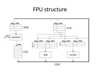
Result • A single core with FPU • FPU wired in through wishbone interface 2
module s1_top ( • sys_clock_i, sys_reset_i, sys_irq_i, • wbm_ack_i, wbm_data_i, • wbm_cycle_o, wbm_strobe_o, wbm_we_o, wbm_addr_o, wbm_data_o, wbm_sel_o • ); • /* • * SPARC Core module instance • */ • sparc sparc_0 ( • ); • /* • * SPARC Core to Wishbone Master bridge • */ • spc2wbm spc2wbm_0 ( • ... • // FPU outputs • .fpu_pcx_req_pq(fpu_pcx_req_pq), • .fpu_pcx_data_pa(fpu_pcx_data_pa) • ); • /* • * dt: adding FPU • */ • fpu fpu_0 ( • .pcx_fpio_data_rdy_px2(fpu_pcx_req_pq), • .pcx_fpio_data_px2(fpu_pcx_data_pa), • .arst_l(cmp_arst_l), • .grst_l(cmp_grst_l), • .gclk(gclk), • .cluster_cken(cluster_cken), • .fp_cpx_req_cq(cpx_fpu_request_px), • .fp_cpx_data_ca(cpx_fpu_data_cx2), • .ctu_tst_pre_grst_l(ctu_tst_pre_grst_l), • .global_shift_enable(global_shift_enable), • .ctu_tst_scan_disable(ctu_tst_scan_disable), • .ctu_tst_scanmode(ctu_tst_scanmode), • .ctu_tst_macrotest(ctu_tst_macrotest), • .ctu_tst_short_chain(ctu_tst_short_chain), • .si(fpu_scanin), • .so(fpu_scanout) • ); • /* • * Reset Controller • */ • rst_ctrl rst_ctrl_0 ( • ); • /* • * Interrupt Controller • */ • int_ctrl int_ctrl_0 ( • ); • endmodule 3
Other problems • Code for most modules have ifdefs for synthesis (FPGA_SYN), Sun’s somewhat custom synthesis (DEFINE_0IN) and a generic synthesis (everything else) • Sun’s code path has some problems • Data cache and instruction cache are incomplete 4
//`ifdef DEFINE_0IN • wire [3:0] dc_we = dcache_wvld_m ? dcache_wr_rway_m : 4'b0; • dc_data dc_data0 ( .nclk(~clk), .adr(dcache_rwaddr_m[10:4]), • .we(dc_we [0] ), .wm(way_mask [143:0]), • .din(dcache_wdata_m[143:0]), .dout(temp_w0a[143:0]) ); • dc_data dc_data1 ( .nclk(~clk), .adr(dcache_rwaddr_m[10:4]), • .we(dc_we [1] ), .wm(way_mask [143:0]), • .din(dcache_wdata_m[143:0]), .dout(temp_w1a[143:0]) ); • dc_data dc_data2 ( .nclk(~clk), .adr(dcache_rwaddr_m[10:4]), • .we(dc_we [2] ), .wm(way_mask [143:0]), • .din(dcache_wdata_m[143:0]), .dout(temp_w2a[143:0]) ); • dc_data dc_data3 ( .nclk(~clk), .adr(dcache_rwaddr_m[10:4]), • .we(dc_we [3] ), .wm(way_mask [143:0]), • .din(dcache_wdata_m[143:0]), .dout(temp_w3a[143:0]) ); • /* • `else 5
Frontend • Using TSMC 0.18um • And SRAM macros Cadence tutorial • 256x16 and 128x16 bit hard macros 7
Synthesis Result • Instance Cells Cell Area Net Area Wireload • ---------------------------------------------------------------------------------------------------- • s1_top 109398 13906100 0 TSMC18_Conservative (D) • sparc_0 86549 13246901 0 TSMC18_Conservative (D) • fpu_0 20987 605398 0 TSMC18_Conservative (D) 8
Backend • I/O: 270 • Area: 21.9 mm^2 • Turns out the SRAM macro 128x16 has same area 256x16 9
Conclusion • Clausewitz: “War is very simple, but in War the simplest things become very difficult.” • Analogy: HW Synthesis is very simple, but in HW Synthesis the simplest things become very difficult. 11