Download
1 / 20
210 likes | 323 Views
Chapter 6 Memory and Programmable Logic Devices. Memory. A collection of cells and logic capable of storing and retrieving binary data -> -> Output Register and C. C. Memory

E N D
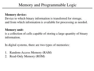
Memory • A collection of cells and logic capable of storing and retrieving binary data • -> -> Output Register and C. C. Memory <- <- Input • RAM (Random Access Memory) - Write operation - Read operation • ROM (Read Only Memory) - Read operation - Programming refers to a hardware process that specifies bits
Programmable Logic Devices (PLD) • ROM • Programmable Logic Array (PLA) • Programmable Array Logic (PAL) • Complex Programmable Logic Devices (C PLD) • Field Programmable Gate Array (FPGA)
Random Access Memory • Word : groups of bits moving in and out of memory as a unit • Byte : 8 bits • Word : multiple of bytes • Random access : the same access time regardless of the location Serial access : different access time e.g., magnetic disk, tape
Memory System Parameter • Capacity : the maximum number of units of data it can store e.g., 2K word, 4 bits/word total = 2 x 1024 x 4 bits • Access time (Read) : the maximum time from the application of an address to the appearance of the data at the Data Output • Data transfer rate (Bandwidth) : the number of bits per second at which the data can be read out ( 1/ access time x the number of bits in an unit ) • Write cycle time : the maximum time from the application of the address to the completion of storing a word Random
Properties of Memory • Static RAM (SRAM) - the stored information remains valid as long as power is applied - internal latches - shorter read/write time - no refresh • Dynamic RAM (DRAM) - store binary information in the form of charges on capacitor - refreshing (read, rewrite) - lower power and larger capacity • Volatile : information lost when power is off Non-volatile
Write and Read Operations • Read : a transfer of a copy of stored word out of memory. 1. Apply the binary address of the desired word to the address lines. 2. Activate Read input Write: a transfer into memory of a new word to be stored. 1. Apply the binary address of the desired word to the address lines. 2. Apply the data bits that must be stored in memory to the data input lines. 3. Activate the Write line. Read/Write signal Chip Select (CS) signal
Programmable Logic Technology Programming technology • Establish or break interconnection - fuse - mask programming - anti-fuse • SRAM bit • Control of transistor switching
VLSI Design • Full custom design • Standard cell design • Gate array • PLD - Complex Programmable Logic Devices (CPLD) - Field Programmable Gate Array (FPGA)
Refresh Type • RAS only refresh. • CAS before RAS refresh. • Hidden refresh
The Control Unit • Control Signals: Load control signals, Selection signals of MUX, bus, ALU • Sequencing: Determine the next state to be activated
Controller • Programmable system - instruction - instruction stored in RAM or ROM - Program Counter (PC) - design example : a simple computer CPU • Non-programmable system: - determine the operations to be performed and the sequence of operations, based on only its inputs and the status bits - design example : Multiplier
Programmable System • A simple computer architecture • Instruction - the ability to execute a program from memory - new data processing performed by * specifying a new program * specifying the same instruction with different data - OP code Data (register, memory, immediate)
Programmable System • A single-cycle instruction • Multiple-cycle instruction - one instruction is executed in many cycles - Instruction fetch Decode Execute Write-back • Pipelined instruction
Algorithm State Machine (ASM) • Hardware algorithm • Similar to a flowchart for software • Different from a flowchart in * relationship to timing: states in response to clock
Implementation of a Controller • Hardwired control * sequence register and decoder * one flip-flop per state • Micro-programmed control * ROM
Micro-programmed Control Design Need to determine • the number of bits in the control word • the structure of the next address generator • the sizes of ROM and CAR
State Transition Table for the Controller See the other file: table
The Structure of the Next Address • Two addresses in the instruction controlling the decision: decision variable = 0 = 1 NXTADD1 NXTADD0 SEL DATAPATH address for decision variable = 0 address for decision variable = 1 • One address and counter