Download
1 / 13
130 likes | 135 Views
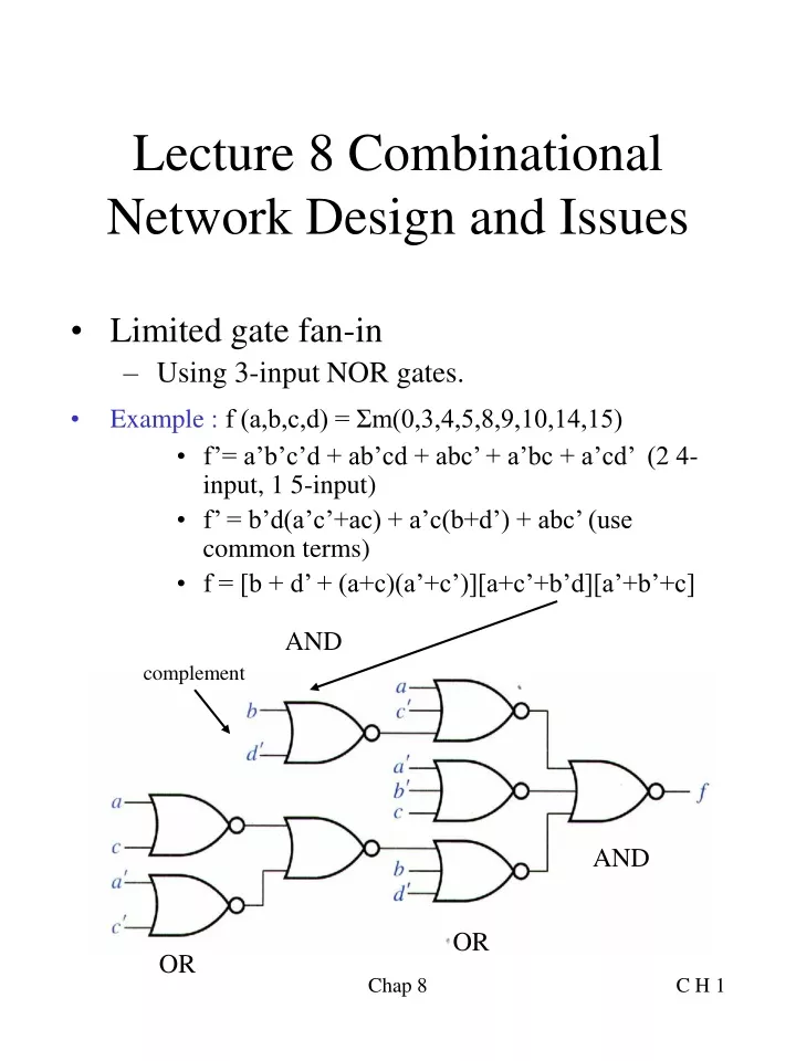
Lecture 8 Combinational Network Design and Issues. Limited gate fan-in Using 3-input NOR gates. Example : f (a,b,c,d) = Σm(0,3,4,5,8,9,10,14,15) f’= a’b’c’d + ab’cd + abc’ + a’bc + a’cd’ (2 4-input, 1 5-input) f’ = b’d(a’c’+ac) + a’c(b+d’) + abc’ (use common terms)

E N D
Lecture 8 Combinational Network Design and Issues • Limited gate fan-in • Using 3-input NOR gates. • Example : f (a,b,c,d) = Σm(0,3,4,5,8,9,10,14,15) • f’= a’b’c’d + ab’cd + abc’ + a’bc + a’cd’ (2 4-input, 1 5-input) • f’ = b’d(a’c’+ac) + a’c(b+d’) + abc’ (use common terms) • f = [b + d’ + (a+c)(a’+c’)][a+c’+b’d][a’+b’+c] AND complement AND OR OR Chap 8
Multiple-Output With Limited Fan-In • Using only 2-input NAND. • f1 = b’c’ + ab’ + a’b • f2 = b’c’ + bc + a’b • f3 = a’b’c + ab + bc’ • 3-input OR-gate • f1 = b’(a+c’) + a’b • f2 = b(a’+c) + b’c’ or (b’+c)(b+c’) +a’b • f3 = a’b’c + b(a+c’) = a’(b+c’)’ + b(a+c’) Choose this because of common term 2 inputs 3 inputs Chap 8
Gate Delay • Propagation delay • Timing diagram Chap 8
Network Delay • Delay element • Extra logic circuit, capacitance. Chap 8
Hazards • Uncertain delays in logic circuits have the ability to introduce temporary or transient signal pulse where none are supposed to exist. • The spurious pulses or noise signals are referred to as glitches. • A glitch is a momentary error condition on the output of a circuit due to unequal signal delay paths in the circuit. • A glitch is identified as an additional pulse or pulses on output. • The circuit conditions that allow such signals to appear are called hazards. • A circuit with a hazard may or may not produce glitches, depending on the input patterns and the electrical charactersitics of the circuit. Chap 8
An Example of Hazard • Propagation delays result in output transients. • When x2 1->0, the output should remain to 1. • But if G1 goes to 1 first, then (11) for G 3 results in 0 output. Suppose that G2 has a longer delay, then (1,0) causes the output back to 1. x2 and x2’ have the same value for a short time. G3 Chap 8
Static and Dynamic Hazard • Hazard • In a combinational part of a sequential network, hazard can cause the sequential network to malfunction. • Hazard in an output network can cause a problem if the output serves as the input to another asynchronous network. Chap 8
Glitch Eliminations • If the glitches are narrow in width, they might be filtered out by the inertial property of physical gates. • Hazard controls are only feasible to fairly small circuits that operate under restrictive conditions. • Avoid multiple simultaneous input changes. (Restriction) Chap 8
Hazard Detection • 1-hazard Chap 8
Remove the Hazard • Add a redundant gate to remove the hazard. Chap 8
Hazard Detection (cont.) • Static 0-hazard Chap 8
Remove Hazard • Looping additional prime implicants that cover the adjacent 0’s that are not already covered by a common loop. Chap 8
Possible Causes for Errors • Incorrect design • Gate connected wrong • Wrong inputs to the network • Defective gates • Defective wires • stuck at zero • stuck at one Chap 8