Download
1 / 24
240 likes | 597 Views
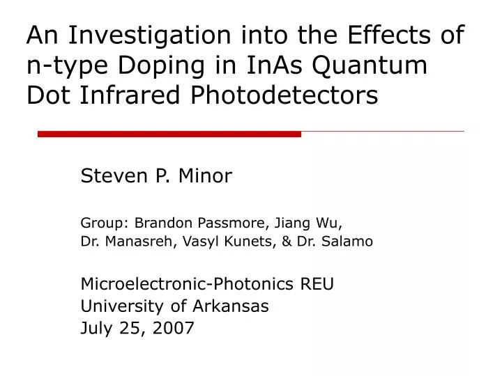
An Investigation into the Effects of n-type Doping in InAs Quantum Dot Infrared Photodetectors. Steven P. Minor Group: Brandon Passmore, Jiang Wu, Dr. Manasreh, Vasyl Kunets, & Dr. Salamo Microelectronic-Photonics REU University of Arkansas July 25, 2007. Presentation Outline.

E N D
An Investigation into the Effects of n-type Doping in InAs Quantum Dot Infrared Photodetectors Steven P. Minor Group: Brandon Passmore, Jiang Wu, Dr. Manasreh, Vasyl Kunets, & Dr. Salamo Microelectronic-Photonics REU University of Arkansas July 25, 2007
Presentation Outline • Introduction to Quantum Dots Infrared Photodetectors (QDIPs), Interband and Intersubband Transitions • Experimental Design • Results • Conclusion • Acknowledgements
Why are QDIPs important? • Two significant advantages over the one dimensionally confined Quantum Well Infrared Photodetector (QWIP) • Can operate at normal incident light due to the three dimensional carrier confinement. • Can operate at near room temperature due to high photoconductive gain and low noise.
What’s a Quantum Dot? • Also known as artificial atoms. • Carriers are confined in three-dimensions. • An example would be InAs grown on GaAs.
Interband Transition • Interband transitions occur when electrons in semiconductor materials absorb photons and are excited from the valence band to the conduction band.
Intersubband Transitions • Intersubband transitions are optical excitations between the quantized energy levels within the conduction band of semiconductor heterostructures.
Different types of Quantum Emission • Field-assisted tunneling occurs when electrons pass through a barrier in the presence of a high electric field. • Thermionic Emission is the flow of charged particles called thermions from a charged metal or a charged metal oxide surface, caused by thermal vibrational energy overcoming the electrostatic forces holding electrons to the surface.
300 nm n-GaAs: Si 2 x 1018 cm-3 50 nm GaAs Spacer 2 ML InAs QDs x10 50 nm GaAs Spacer 500 nm n-GaAs: Si 2 x 1018 cm-3 S.I. GaAs (100) Substrate Growth Objectives • Vary carrier concentrations in the Quantum Dots • Control Sample: Undoped • Dependent Samples: • 1 x 1017 cm-3 • 5 x 1017 cm-3 • 1 x 1018 cm-3
Measurement Equipment • Doping Concentrations • Accent Electrochemical Capacitance-Voltage Pro • Photoluminescence • Bomem Fourier-transform Infrared Spectrometer • Current-Voltage • Keithley Semiconductor Characterization system • Photoresponse • Bruker Fourier-transform Infrared Spectrometer • Standford Research System low-noise preamplifier
Results • ECV
Results • Photoluminescence
Results • Dark Current • Measured at 77 K
Results • Photoresponse • Measured at 77 K.
Results • Atomic Force Microscope (AFM)
Results • Used a computer program to detect dots and calculate the average quantum dot density per cm2. • Averages • Dot Height: 5 nm • Lateral Diameter: 28 nm • Dot Density: 2.44 x 1010 cm-2
Results • Optimal Photoresponse was observed from the sample in which the carrier concentration donated 2 electrons per dot.
Conclusion • Introduced to graduate level research • Learned about nanostructures and infrared photodetectors • Experimentally verified previous research results
Acknowledgements • Dr. Manasreh • Brandon Passmore • Jiang Wu • Vasyl Kunets • Eric Decuir • Dr. Salamo • Ken Vickers and Renee Hearon
References • B. F. Levine, “Quantum well infrared photodetectors,” J. Appl. Phys.,vol. 74, p. R1, 1993. • M. O. Manasreh, Semiconductor Heterojunctions and Nanostructures. New York: McGraw-Hill, 2005, ch. 10, pp. 457–528. • Shih-Yen LIN, Yao-Jen TSAI and Si-Chen LEE, “Effect of Silicon Dopant on the Performance of InAs/GaAs Quantum-Dot Infrared Photodetectors,” Japanese J. Appl. Phys., Vol. 43, No. 2A, 2004, pp. L 167–L 169 • J. Phillips, K. Kamath, X. Zhou, N. Chervela, and P. Bhattacharya, “Photoluminescence and far-infrared absorption in Si-doped self-organized InAs quantum dots,” Appl. Phys. Lett. 71(15), 13 October 1997. • A. D. Stiff-Roberts, X. H. Su, S. Chakrabarti, and P. Bhattacharya,” Contribution of Field-Assisted Tunneling Emission to Dark Current in InAs–GaAs Quantum Dot Infrared Photodetectors,” IEEE PHOTONICS TECHNOLOGY LETTERS, VOL. 16, NO. 3, MARCH 2004. • Jie Liang, Ying Chao Chua, M. O. Manasreh, Euclydes Marega, Jr., and G. J. Salamo, “Broad-Band Photoresponse From InAs Quantum Dots Embedded Into InGaAs Graded Well,” IEEE ELECTRON DEVICE LETTERS, VOL. 26, NO. 9, SEPTEMBER 2005.