Download
1 / 30
300 likes | 310 Views
Recovery-Driven Design: A Power Minimization Methodology for Error-Tolerant Proces s or Modules. Andrew B. Kahng † , Seokhyeong Kang † , Rakesh Kumar ‡ and John Sartori ‡ † VLSI CAD LABORATORY, UCSD ‡ PASSAT GROUP, UIUC DAC, June 17, 2010. Outline. Background and Motivation

E N D
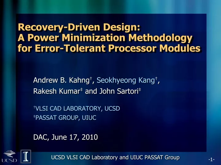
Recovery-Driven Design: A Power Minimization Methodology for Error-Tolerant Processor Modules Andrew B. Kahng†, Seokhyeong Kang†, Rakesh Kumar‡ and John Sartori‡ †VLSI CAD LABORATORY, UCSD ‡PASSAT GROUP, UIUC DAC, June 17, 2010
Outline • Background and Motivation • Voltage scaling and error-tolerant design • Error-tolerant design vs. recovery-driven design • Recovery-Driven Design • Related work • Heuristic: power minimization • Error rate estimation • Experimental Framework and Results • Design methodology • Results and analysis • Conclusions and Ongoing Work
Reducing Power with Voltage Scaling • Power is a first-order design constraint • Moore’s law implies power density of processors continues to escalate • Voltage scaling reduces power but eventually causes massive timing violations Voltage Timing errors begin to occur • Error-resilience allows deeper voltage scaling
Error-Tolerance Mechanisms • Hardware error-tolerance • Errors are detected and corrected during runtime • Razor (MICRO 2003) • Application-level error-tolerance* • Errors are allowed to propagate to software resulting in reduced performance or output quality Traditional IC design Error-Tolerant design • No errors allowed • Error correction architecture allows timing errors • Overclockingand voltage overscalingnot enabled • Overclocking and voltage overscaling enabled *Hedge et al. “Energy-Efficient Signal Processing via Algorithmic Noise-Tolerance”, ISLPED 1999
Our Work: From Error-Tolerance to Recovery-Driven Error-Tolerant design Recovery-Driven design • Design still optimized for correct operation • Design methodology based on STA, workload-agnostic • Designed “from ground up” for specific target error rate • Design methodology exploits functional information
Recovery-Driven Design 1. Minimize error rate to extend range of voltage scaling How to minimize power in recovery-driven design? 2. Reduce design power with cell downsizing or Vt swap Error rate (traditional) Error rate (optimized) Error rate Power 1. OptimizePaths Operating point New operating point Pmin Target error rate Pmin Power (traditional) Power (optimized) 2. ReducePower Vmin Vmin lower voltage
Outline • Background and motivation • Voltage scaling and error-tolerant processor • Error-tolerant design vs. recovery-driven design • Recovery-Driven Design • Related work • Heuristic: power minimization • Error rate estimation • Experimental Framework and Results • Design methodology • Results and analysis • Conclusions and Ongoing Work
Related Works: Design-Level Optimizations for Error-Tolerant Processors • BlueShift* • Increase frequency up to a target error rate • Speed up error paths with timing overrides and FBB • Slack Optimizer** • Make gradual slope slack to achieve gracefully increasing error rate • Estimate error rate using switching activity from SAIF *Grescamp et al. “Blueshift: Designing Processors for Timing Speculation from the Ground up”, HPCA 2009 **Kahng et al. “Slack Redistribution for Graceful Degradation Under Voltage Overscaling”, ASPDAC 2010
Recovery-Driven Design Methodology • Problem: minimize processor power (leakage + dynamic) for a target error rate • Approach: we use slack redistribution and power reduction enabled by accurate error rate estimation • Slack redistribution: reshape path slack based on path activity (toggle rate) to minimize error rate and extend voltage scaling (OptimizePathsand ReducePowerheuristics) • Error rate estimation using a simulation dump file (VCD)
Slack Redistribution • Redistribute slack from paths that rarely toggle to paths that frequently toggle OptimizePaths ReducePower
Slack Redistribution Flow • Toggle Information:simulation dump file is loaded • Path Optimization: minimize error rate to extend range of voltage scaling • Power Reduction: downsize cells to obtain additional power savings • Error Rate Estimation: estimate with toggle info and STA results Netlist VCD Analyze activity Timing Analysis OptimizePaths ReducePower Reduce Voltage ERCompute Error Rate ER > ERtarget NO YES ECO P&R
Heuristic Details – OptimizePaths • OptimizePaths→ ReducePower → Voltage Scaling • Main idea: increase slack of frequently-exercised paths in order of decreasing toggle rate • Procedure • Pick a critical path p with maximum toggle rate • Resize cell instance ci in p • If the path slack is not improved, cell change is restored • Repeat 2. ~ 3. for all cell instances in path p • Repeat 2.~ 4. for all critical paths
Heuristic Details – ReducePower • OptimizePaths→ ReducePower→ Voltage Scaling • Main idea: downsize cells on non-critical paths in order of decreasing sensitivity • Sensitivity (c) = (powerc – powerc’) / (slackc – slackc’) • Procedure • Pick a cell c with maximum sensitivity • Downsize cell c with logically equivalent cell • Incremental timing analysis and check error rate • If error rate is increased, cell change is restored • Repeat 1. ~ 4.
Path Extraction for Error Rate Estimation • Instead of simulation, we use toggle information from value change dump (VCD) file List of toggled netsin each cycle time
Toggle and Error Rate Calculation • 20Xfaster than actual simulation and accurate p: path χtoggle: set of cycles which p has toggled Xtot: total cycle # • Toggle rate: • Error rate: *Kahng et al. “Slack Redistribution...”, ASPDAC 2010.
Evaluation of Heuristic Design Choices • Path ordering • toggle rate * slack • toggle rate • Optimization radius • path only • fan-in/out network • Starting netlist • loosely constrained • tightly constrained • Voltage step size • 0.01V and 0.05V
Outline • Background and motivation • Voltage scaling and error-tolerant processor • Error-tolerant design vs. recovery-driven design • Recovery-Driven Design • Related work • Heuristic: power minimization • Error rate estimation • Experimental Framework and Results • Design methodology • Results and analysis • Conclusions and Ongoing Work
Design Methodology • System level simulation using Simics with real benchmarks • Gate level simulation to get signal toggle information (NC verilog) • Prepare Synopsys Liberty file using Cadence Signal Storm • Implement in C++ and use Tcl socket to communicate with PrimeTime • Perform ECO P&R with cell swap list
Power Analysis for Real Workloads input pattern system-level simulation Simics + Transplant functional simulation VCS or NCVerilog VCD design implementation DC, SOCE netlist SPEF power analysis PrimeTime-PX RTL design OpenSPARC benchmark binary (bzip, twolf ...) memory modeling MEMGEN, CACTI Liberty (.lib) • System level simulation with real benchmark binary and input patterns are captured • Estimate power of memory – MEMGEN, CACTI • Analyze leakage and dynamic power using PT-PX
Testbed • Target design: sub-modules of OpenSPARC T1 • Benchmark: ammp, bzip2, equake, twolf, sort.Fast-forward, capture vectors • Implementation: TSMC 65GP technology with standard SP&R • Alternative design techniques: • SP&R with loose constraints and tight constraints • Slack Optimizer (make a “gradual slope”) [ASPDAC2010]
Power Consumption of Each Design Technique • Power savings compared to tradition SP&R design 25% power savings @ 0.125% error rate (average) LSU_STB_CTL Error rate (%) • Area overhead and power savings (from loose SP&R)
Power Consumption for HW-Based Error Tolerance • Razor architecture was assumed for error detection and correction – account for Razor overhead (area, power) and power cost of error correction LSU_STB_CTL 21% additional power savings 0.84V 0.76V
Conclusions and Ongoing Work • We propose recovery-driven design which minimizes power for a target timing error rate • Optimize designs with functional information and iterative voltage scaling • We also develop a fast and accurate technique for post-layout activity and error rate estimation • We demonstrate significant power benefits – up to 25% power savings compared to traditional P&R at an error rate of 0.125% • Ongoing work • Recovery-driven design for different error resilience mechanisms, different sources of variation • Design / architecture co-exploration
Related Work: BlueShift • BlueShift* : maximize frequency for a given error rate • BlueShift speedup • Paths with the highest frequency of timing errors • FBB (forward body-biasing) & Timing override • Limitation • Repetitive gate level simulation – impractical • Design overhead of FBB ER < Target NO Compute error rate Speed up paths Gate-level simulation YES Finish *Grescamp et al. “Blueshift: Designing processors for timing speculation from the ground up”, HPCA 2009
Exploiting Error Resilience for Multi-core Design • Design of heterogeneously reliable multi-core processor • Power-optimized for different reliability target • Power-optimized for different mixes of workloads Individual cores are customized for a specific workload class
Lifetime Energy Minimization • Maximizing energy efficiency of DVFS-based designs • Inefficiency is due to a design optimized for a single power / performance point • Minimize energy when the processor spends R of its lifetime at high freq. (e.g., talk mode) and (1 – R) of its lifetime at low freq. (e.g., standby mode) • Replication-based methodology: area overhead vs. power tradeoffs • Co-optimization methodology: optimize design with two operating constraints – (freq_hi, V_hi) and (freq_lo, V_lo) • Both methodologies can be applied alternatively in each sub-modules
Sensitivity-Based Optimization Platform • Post-layout stage cell swap • Cell sizing + ECO • Multi-Vt swap • Multi-Lgate swap • Swap cell and check STAwith PrimeTime socketinterface • Cell swap according to the sensitivity S • For leakage optimization, S = Δleakage x slack • For timing closure, S = Δslack / (slack – WNS) • MMMC (Multi-Mode Multi-Corner) can be considered with multiple PrimeTime sockets Lgate biasing
Limitations of Traditional CAD Flow • In modern digital design, vast majority of paths have near-critical slack – wall of slack distribution • Scaling beyond a critical operating point causes massive errors and power benefits can be limited* # cycles which have timing error number of paths ‘wall of slack’ error rate Error rate = # total cycles 20.0 %at 0.90V 0.0 %at 1.00V 1.0 %at 0.95V timing slack lower voltage (higher frequency) operating point zero slack *Kahng et al. “Slack Redistribution...”, ASPDAC 2010.