Download
1 / 1
10 likes | 102 Views
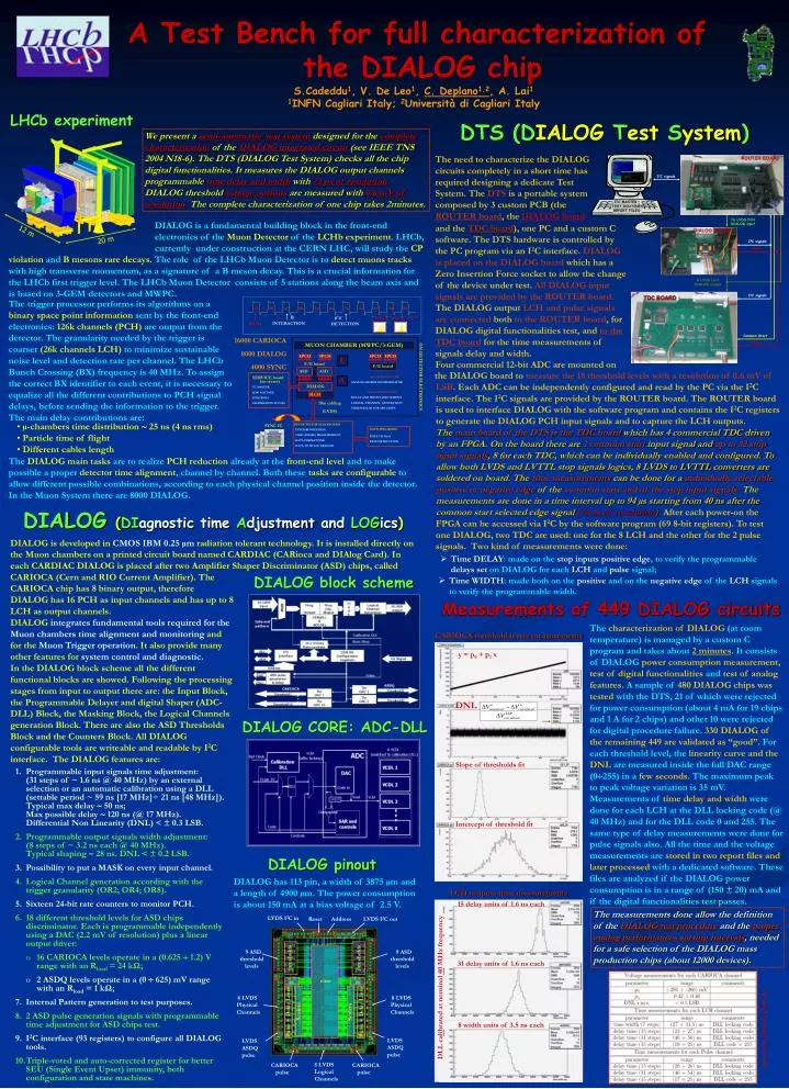
thresholds. thresholds. DLL ADC. core. DLL ADC. 8PCH. 8PCH. 8PCH. 8PCH. gnd. gnd. gnd. gnd. gnd. gnd. gnd. gnd. gnd. gnd. ASD. ASD. Scalers. Pulse + Delay Lines. Scalers. Pulse + Delay Lines. vdd. vdd. vdd. vdd. vdd. vdd. vdd. vdd. vdd.

E N D
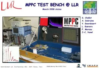
thresholds thresholds DLL ADC core DLL ADC 8PCH 8PCH 8PCH 8PCH gnd gnd gnd gnd gnd gnd gnd gnd gnd gnd ASD ASD Scalers Pulse + Delay Lines Scalers Pulse + Delay Lines vdd vdd vdd vdd vdd vdd vdd vdd vdd vdd 25 ns 25 ns 25 ns I2C signals ROUTER BOARD I2C MASTER TEST ROUTINES REPORT FILES 12 m 16 LVDS PCH DIALOG input 20 m I2C signals 45 46 47 48 49 50 51 52 53 54 55 Reset B m+m- INTERACTION BX ID DETECTION TDC BOARD 8 LVDS LCH DIALOG output MUON CHAMBER (MWPC/3-GEM) DIALOG BOARD I2C signals F/E board F/E board SERVICE board ASD: CARIOCA CHIP ANALOG SHAPER DISCRIMINATOR ON DETECTOR ELECTRONICS (on crates) DIALOG I2C MASTER LOW VOLTAGE CONTROLS CALIBRATION PULSES DIALOG CUSTOM IC DELAY AND WIDTH ADJUSTMENT LOGICAL CHANNEL GENERATION THRESHOLDS FOR ASD CHIPS 8LCH Common Start 10m cabling (LVDS) Reset OFF DETECTOR ELECTRONICS SYNCHRONIZATION TIME (PHASE) MEASUREMENT DATA FORMATTING DATA TO MUON TRIGGER SYNC IC COUNTING ROOM DATA TO DAQ RECONSTRUCTION DIALOG block scheme y = p0 + p1 x DNL Slope of thresholds fit Intercept of threshold fit LCH outputs time measurements 15 delay units of 1.6 ns each LVDS I2C in Reset Address LVDS I2C out 9 ASD threshold levels 9 ASD threshold levels 31 delay units of 1.6 ns each DLL calibrated at nominal 40 MHz frequency 8 LVDS Physical Channels 8 LVDS Physical Channels 8 width units of 3.5 ns each LVDS ASDQ pulse LVDS ASDQ pulse 8 LVDS Logical Channels CARIOCA pulse CARIOCA pulse A Test Bench for full characterization of the DIALOG chip S.Cadeddu1, V. De Leo1, C. Deplano1,2, A. Lai1 1INFN Cagliari Italy; 2Università di Cagliari Italy LHCb experiment DTS (DIALOG Test System) We present a semi-automatic test system designed for the complete characterization of the DIALOG integrated circuit (see IEEE TNS 2004 N18-6). The DTS (DIALOG Test System) checks all the chip digital functionalities. It measures the DIALOG output channels programmable time delay and width with 72 ps of resolution. DIALOG threshold voltage outputs are measured with 0.6 mV of resolution. The complete characterization of one chip takes 2minutes. The need to characterize the DIALOG circuits completely in a short time has required designing a dedicate Test System. The DTS is a portable system composed by 3 custom PCB (the ROUTER board, the DIALOG board DIALOG is a fundamental building block in the front-end electronics of the Muon Detector of the LCHb experiment. LHCb, currently under construction at the CERN LHC, will study the CP and theTDC board), one PC and a custom C software. The DTS hardware is controlled by the PC program via an I2C interface. DIALOG is placed on the DIALOG board which has a Zero Insertion Force socket to allow the change of the device under test. All DIALOG input signals are provided by the ROUTER board. The DIALOG output LCH and pulse signals are connected both to the ROUTER board, for DIALOG digital functionalities test, and to the TDC board for the time measurements of signals delay and width. Four commercial 12-bit ADC are mounted on violation and B mesons rare decays. The role of theLHCb Muon Detectoris to detect muons tracks with high transverse momentum, as a signature of a B meson decay. This is a crucial information for the LHCb first trigger level. The LHCb Muon Detector consists of 5 stations along the beam axis and is based on 3-GEM detectors and MWPC. The trigger processor performs its algorithms on a binary space point information sent by the front-end electronics: 126k channels (PCH) are output from the detector. The granularity needed by the trigger is coarser (26k channels LCH) to minimize sustainable noise level and detection rate per channel. The LHCb Bunch Crossing (BX) frequency is 40 MHz. To assign the correct BX identifier to each event, it is necessary to equalize all the different contributions to PCH signal delays, before sending the information to the trigger. The main delay contributions are: 16000 CARIOCA 8000 DIALOG 4000 SYNC the DIALOG board to measure the 18 threshold levels with a resolution of 0.6 mV of LSB. Each ADC can be independently configured and read by the PC via the I2C interface. The I2C signals are provided by the ROUTER board. The ROUTER board is used to interface DIALOG with the software program and contains the I2C registers to generate the DIALOG PCH input signals and to capture the LCH outputs. The main board of the DTS is the TDC board which has 4 commercial TDC driven by an FPGA. On the board there are 1 common start input signal and up to 32 stop input signals, 8 for each TDC, which can be individually enabled and configured. To allow both LVDS and LVTTL stop signals logics, 8 LVDS to LVTTL converters are soldered on board. The time measurements can be done for a individually selectable positive or negative edge of the common start and of the stop input signals. The measurements are done in a time interval up to 94 µs starting from 40 ns after the common start selected edge signal (72 ns of resolution). After each power-on the FPGA can be accessed via I2C by the software program (69 8-bit registers). To test one DIALOG, two TDC are used: one for the 8 LCH and the other for the 2 pulse signals. Two kind of measurements were done: • µ-chambers time distribution 25 ns (4 ns rms) • Particle time of flight • Different cables length The DIALOG main tasks are to realize PCH reduction already at the front-end level and to make possible a proper detector time alignment, channel by channel. Both these tasks are configurable to allow different possible combinations, according to each physical channel position inside the detector. In the Muon System there are 8000 DIALOG. DIALOG (DIagnostictimeAdjustmentand LOGics) DIALOG is developed in CMOS IBM 0.25 µm radiation tolerant technology. It is installed directly on the Muon chambers on a printed circuit board named CARDIAC (CARioca and DIAlog Card). In each CARDIAC DIALOG is placed after two Amplifier Shaper Discriminator (ASD) chips, called • Time DELAY: made on the stop inputs positive edge, to verify the programmable delays set on DIALOG for each LCH and pulse signal; CARIOCA (Cern and RIO Current Amplifier). The CARIOCA chip has 8 binary output, therefore DIALOG has 16 PCH as input channels and has up to 8 LCH as output channels. DIALOG integrates fundamental tools required for the Muon chambers time alignment and monitoring and for the Muon Trigger operation. It also provide many other features for system control and diagnostic. In the DIALOG block scheme all the different functional blocks are showed. Following the processing stages from input to output there are: the Input Block, the Programmable Delayer and digital Shaper (ADC-DLL) Block, the Masking Block, the Logical Channels generation Block. There are also the ASD Thresholds Block and the Counters Block. All DIALOG configurable tools are writeable and readable by I2C interface. The DIALOG features are: • Time WIDTH: made both on the positive and on the negative edge of the LCH signals to verify the programmable width. Measurements of 449 DIALOG circuits The characterization of DIALOG (at room temperature) is managed by a custom C program and takes about 2 minutes. It consists of DIALOG power consumption measurement,test of digital functionalities and test of analog features. A sample of 480 DIALOG chips was tested with the DTS, 21 of which were rejected for power consumption (about 4 mA for 19 chips and 1 A for 2 chips) and other 10 were rejected for digital procedure failure. 330 DIALOG of the remaining 449 are validated as “good”. For each threshold level, the linearity curve and the DNL are measured inside the full DAC range (0255) in a few seconds. The maximum peak to peak voltage variation is 35 mV. Measurements of time delay and width were done for each LCH at the DLL locking code (@ 40 MHz) and for the DLL code 0 and 255. The same type of delay measurements were done for pulse signals also. All the time and the voltage measurements are stored in two report files and later processed with a dedicated software. These files are analyzed if the DIALOG power consumption is in a range of (150 ± 20) mA and if the digital functionalities test passes. CARIOCA threshold levels measurements DIALOG CORE: ADC-DLL • Programmable input signals time adjustment: (31 steps of ~ 1.6 ns @ 40 MHz) by an external selection or an automatic calibration using a DLL (settable period ~ 59 ns [17 MHz]÷ 21 ns [48 MHz]). Typical max delay 50 ns; Max possible delay 120 ns (@ 17 MHz). Differential Non Linearity (DNL) < ± 0.3 LSB. • Programmable output signals width adjustment: (8 steps of ~ 3.2 ns each @ 40 MHz). Typical shaping 28 ns. DNL < ± 0.2 LSB. • Possibility to put a MASK on every input channel. • Logical Channel generation according with the trigger granularity (OR2; OR4; OR8). • Sixteen 24-bit rate counters to monitor PCH. • 18 different threshold levels for ASD chips discriminator. Each is programmable independently using a DAC (2.2 mV of resolution) plus a linear output driver: • 16 CARIOCA levels operate in a (0.625 1.2) V range with an Rload = 24 kΩ; • 2 ASDQ levels operate in a (0 625) mV range with an Rload = 1 kΩ; • Internal Pattern generation to test purposes. • 2 ASD pulse generation signals with programmable time adjustment for ASD chips test. • I2C interface (93 registers) to configure all DIALOG tools. • Triple-voted and auto-corrected register for better SEU (Single Event Upset) immunity, both configuration and state machines. DIALOG pinout DIALOG has 113 pin, a width of 3875 µm and a length of 4900 µm. The power consumption is about 150 mA at a bias voltage of 2.5 V. The measurements done allow the definition of the DIALOG test procedure and the proper analog performances sorting intervals, needed for a safe selection of the DIALOG mass production chips (about 12000 devices). Analog Sorting Intervals