Download
1 / 15
150 likes | 442 Views
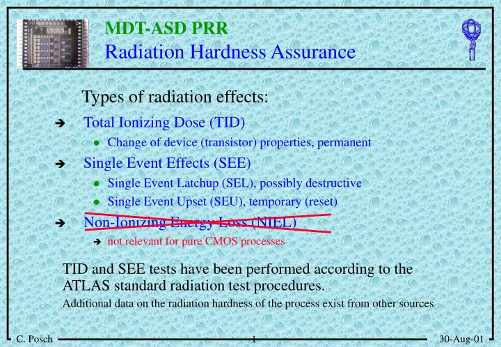
Total Ionizing Dose (TID) Change of device (transistor) properties, permanent Single Event Effects (SEE) Single Event Latchup (SEL), possibly destructive Single Event Upset (SEU), temporary (reset) Non-Ionizing Energy Loss (NIEL) not relevant for pure CMOS processes.

E N D
Total Ionizing Dose (TID) Change of device (transistor) properties, permanent Single Event Effects (SEE) Single Event Latchup (SEL), possibly destructive Single Event Upset (SEU), temporary (reset) Non-Ionizing Energy Loss (NIEL) not relevant for pure CMOS processes Radiation Hardness Assurance Types of radiation effects: TID and SEE tests have been performed according to the ATLAS standard radiation test procedures. Additional data on the radiation hardness of the process exist from other sources
Total Ionizing Dose (TID) test Radiation Facility: • Harvard Cyclotron • 160 MeV proton beam, variable fluence up to 3·1010 p/sec • Beam diameter adjustable from 0.1 cm to 30 cm Beam Setup and dose calculation: • 4.41·108 p/cm2 per Monitor Unit (MU) • Ionizing dose in Silicon: 30.21 rad(Si)/MU. • 2.38 MU/sec yields a dose rate of ~ 70 rad/sec. DUT and total dose : • 10 devices were irradiated to a TID of 302 krad • 5 non-irradiated devices characterized for comparison
TID test setup Online monitored DC parameters: • On-chip bias generator voltages • Pre-amp input levels • LVDS output levels • Power consumption All values are displayed on screen for immediate observation and are also recorded with the proper timing information for offline analysis During irradiation the DUT is biased and run under its nominal operating conditions, however there are no signals passed through the analog amplifier chain. The digital part is exercised periodically
Results - DC parameters (I) The observed changes in DC parameters appeared very similar on all of 10 irradiated devices so only the averages across all DUTs are plotted. • Pre-amp bias voltages dropped between 2% (Vb4) and 5% (Vb3) • Pre-amp input DC levels dropped by 3% - 4%.
Results - DC parameters (II) • The DC levels of the LVDS output drivers drop 2% - 3% • There was no measurable increase in power consumption - no noticeable radiation induced leakage current increase occurred
Comparison to Gamma Radiation Data Gamma irradiation of ASD00A at the CERN X-ray facility • 30 keV gammas • TID of 1 Mrad • Steps: 10k, 50k, 100k, 300k, 1Mrad • Dose rate: ~ 170 rad/sec Parameter Gammas Protons Wilk. jitter increase 118 ps 91 ps Time error increase 25 ps 28 ps Amp gain decrease 15.4 mV 15.3 mV
Gamma TID results • The averaged RMS timing error increases by 7 % after 300 krad TID • At the RTCtid for ASIC qualification, the RMS timing error increase is negligible • The voltage gain of the complete analog signal chain - pre-amp, shaper (3 diff amps), analog pad driver drops by 5 % after 300 krad TID • At RTCtid the gain drop of the full chain is of the order of 1 % • The chip is fully functional after 1 Mrad with a gain drop of 18 % and a timing error increase of 15 %
HP 0.5m CMOS process: TID tolerance “Total Dose Hardness …”: (Osborne et. al., IEEE Trans. Nucl. Sci., 1998) (Paul O`Connor, BNL, 1999) CSC-ASD (similar circuit), 60Co irradiation Results (1 Mrad): • increase in supply current negligible, almost no radiation induced leakage current. • Gain drop: 4.06 -> 3.99 mV/fC (- 1.5 %) • Noise increase: 1750 -> 2050 rms e- ENC (+ 17 %) • No wave-form change “The best TID radiation tolerance is achieved in the HP 0.5m process. The average change in threshold voltage at 100 krad is less than 40 mV for the n-channel and less than 20 mV for the p-channel devices.” “The HP 0.5 m process appears to be a candidate for missions with a total dose requirement of 100 krad.”
Single Event Effect (SEE) test Radiation Facility: • Harvard Cyclotron • 160 MeV proton beam Beam Setup and Fluence: • 1.05·109 p ·cm-2 ·s-1 • 1.7 cm beam diameter • 10 devices up to a fluence 4.4·1012 p·cm-2 per device • Total fluence 4.46·1013 p·cm-2 • For Single Event Upset (SEU) monitoring the test system periodically reads all on-chip register contents, compares them to an initial state and re-writes the registers. • Every bit flip is recorded and time stamped. The period of this read-write cycle is approximately 3 seconds. • The power consumption of the DUT is monitored to catch Single Event Latchups (SEL). • During irradiation the DUT is biased and run under its nominal operating conditions, however there are no signals passed through the analog amplifier chain.
SEE Test Results • 7 SEUs (bit flips) were observed after 4.46·1013 protons·cm-2 • 4 SEUs in the shift register, 3 SEUs in the setup register • No hard/destructive SEEs (stuck bits, latch-ups) occurred
SEU - impact calculation • Proton irradiation of 10 devices up to a total fluence of 4.46·1013p·cm-2yielded enough statistics to make a solid prediction on average fluence per SEE per device. • The relevant numbers are 0.2 SEUs per devicein 10 years and 2.4 SEUs per day for all of ATLAS. No hard/destructive SEE (e.g. latch-ups) occurred. • The worst case impact of one SEU is the loss of 8 channels out of 360'000 for the time of one update interval. • Occurence probability of 1 out of 53 SEUs or approximately once per month. • The SEU rate is very manageable and will not cause any considerable degradation in performance of the ATLAS MDT detector.
HP 0.5m CMOS process: SEL tolerance “Single Event Latchup …”: (Osborn et. al.7th NASA Symposium on VLSI design, 1998) Conservative design rules: (MOSIS SCMOS) Double Min. Well-to-Active spacing: 3m 81 LET latchup threshold “A recent simulation study [Huthinen et al.] has shown that the maximum energy deposition occurring with non-negligible probability in the LHC radiation environment will correspond locally to a LET lower than 50 MeVcm2mg-1.” (Extremely rare “worst-case” assumption)
CMOS Latchup - Well-to-Active Spacing Well-to-Active spacing 3m p-substrate Rwell Rsub
Total Ionizing Dose (TID) ASD fully functional after ionizing dose corresponding to 17 times worst case RTC (1 DUT) and ~ 5 times RTC (10DUTs) No measurable increase in supply current radiationinduced leakage current insignificant Device parameter changes at expected maximum dose completely negligible Single Event Effects (SEE) Single Event Upset (SEU) Worst case SEU expected at a rate of ~ 1 per month Hard/destructive SEE: No occurance Single Event Latchup (SEL): Process tested for SEL - critical LET not expected in LHC ASD radiation tolerance: Summary