Download
1 / 13
130 likes | 256 Views
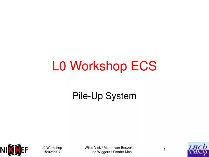
L0 Workshop ECS. Pile-Up System. ECS interface overview. ECS Control hierarchy. ECS. CU. DAI. HV. DCS. DAQ. CCPC. SPECS. Optical station Crate. Bias HV sensors. temp sens. hybrids. VELO ctrl Boards. Analog TELL1. Analog TELL1. Analog TELL1. Vertex Pro. crate. Analog TELL1.

E N D
L0 Workshop ECS Pile-Up System 1
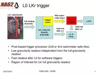
ECS Control hierarchy ECS CU DAI HV DCS DAQ CCPC SPECS Optical station Crate Bias HV sensors temp sens. hybrids VELO ctrl Boards Analog TELL1 Analog TELL1 Analog TELL1 Vertex Pro. crate Analog TELL1 Optical-Tx Brd DU Optical-Tx Brd Optical-Tx Brd VEPROB Hybrids Power supply hybrid1 Dig. TELL1 Optical-Tx Brd VEPROB hybrid2 hybrid3 Optical-Tx Brd VEPROB hybrid4 Optical-Tx Brd VEPROB Output Board Optical-Tx Brd Optical-Tx Brd 3
Connected Device Units • PVSS connected to hardware drivers (DAQ) • VELO control board • 2 or 3 boards each: one SPECS slave • Controlled by one SPECS Master • VEPROB • 4 boards each: one CCPC • Output Board • 1 board: one CCPC • Optical TELL1 • 1 board: one CCPC • Analog TELL1 • 4 boards each: one CCPC • Total connected to hardware drivers • 1 SPECS Master • 10 CCPC’s 4
Sub-system or Sub-detector ? Detector DAQ hybrid1 • Pile-Up in 2 DAQ domains • Sub-system: TPU • Sub-detector: PU • 2 or 3 VELO control boards • 2 boards: • Separated left and right detector, same as VELO structure • Control boards in shared domains • 3 boards: • Extra slot in crate • Different configured VELO control boards • No left/right symmetry detector • Better separation between ECS domains • One specs slave on VELO control board shared by hybrids (detector) and Optical Tx Boards (system) • Can one VELO control board be part of two ECS hierarchies • Analog TELL1 Detector/System? • VELO analog TELL1 => sub-detector • Possible all devices in sub-system TPU with 2 VELO control boards? hybrid2 ? DAQ Optical-Tx Brd VELO Ctrl board Optical-Tx Brd Optical-Tx Brd Optical-Tx Brd System DAQ Analog data-path => Sub-system DAQ Analog TELL1 hybrids Digital data-path => Sub-system DAQ Processing Digital TELL1 hybrids 5
Hybrid • Configuration via SPECS on VELO Control Board -> I2C • FSM: DAQ Domain • 4 hybrids, each: • 16 Beetles, each: • 18 Bytes registers • 2 X 16 Byte registers • 128 Bytes comparator thresholds (additional to VELO hybrids) • Total: ~ 11k Byte • Configuration time: seconds • PVSS software by VELO group • Maybe small modifications for comparator specific registers 6
Optical station • Configuration via SPECS on VELO control board -> I2C • FSM: DAQ Domain • 8 Optical Tx Boards, each: • 12 GOL, each: • 5 Byte config/stat registers • 3 FPGA Sync/Mux logic, each: • EEPROM based (not configurable via ECS) • 32 Byte data sync registers • 12 bit Bcid offset • 16 Byte conf,status,SEU & debug registers • Total: ~ 2k Bytes • Configuration time: < 1second • PVSS Software by Pile-Up group 7
VEPROB • Configuration via CCPC -> I2C/Local bus/JTAG • FSM: DAQ Domain (long conf.) • 4 Vertex processor boards, each: • 20 Byte TTCrx registers • 32 Mbit FPGA conf (per det. pos.) • 18MByte STAPL (per detector position) • 4 events X 2kbit testpatterns • 12 X 4 Byte control/debug/status registers • 24 X 4 Byte optical link status registers • 2 X 1 Byte threshold registers • Total: 1190 Bytes (registers & debug RAM) • Total: 18MByte (FPGA configuration) • FPGA configuration time: • Jam player STAPL 10 minutes (PROM) • PROM preloaded, config cmd: 500 ms • Register Configuration time: < 1 second • PVSS software by Pile-Up group 8
Output Board • Configuration via CCPC -> Local bus / JTAG • FSM: DAQ Domain • Output board • 16 Mbit FPGA Configuration • 16 Byte Control status & debug registers • 80 kByte Histograms • Readout via CCPC into PVSS ?? • Total: ~ 80kByte register & histogram RAM • Total: 16 Mbit FPGA configuration • Register/RAM Configuration time: < 1 second • FPGA Configuration time: many seconds (tbd) • PVSS software by Pile-Up group 9
VELO Control Board • 3 VELO control boards used in Pile-Up • 2 VCB for 8 Optical tx Boards • 1 VCB for 4 hybrids • FSM: DAQ Domain • Per control board • FPGA configuration EEPROM based (not configurable via ECS?) • TTCrx settings • 20 Bytes Clock delay • 6 Delay25 chips • 6 Bytes each • SPECS Slave • ? Bytes • FPGA control registers • ? Bytes • Hybrid temperature monitoring • ? Bytes • PVSS software by VELO group 10
TELL1 • Analog TELL1 • Identical to VELO • PVSS software by VELO • Digital TELL1 • Pile-Up specific • PVSS software: • Based on other TELL1 PVSS software • Modifications by Pile-Up group 11
FSM: Other domains • DAQ & trigger infrastructure (DAI) • Power Supply of processor crate • Standard LHCb crate (standard software?) • PS of optical station crate • Maraton supply (standard software?) • PS of hybrids • Identical to VELO hybrid PS (copy of VELO software) • Detector infrastructure (DCS) • Temperature sensors on hybrid/repeater cards • Identical to VELO • High Voltage (HV) • Bias of silicon sensors • Identical to VELO 12
PVSS panels • Hybrid • Panels • Beetle settings • PVSS panels by VELO group • Comparator threshold added by Pile-Up group • VELO Control Board • Panels • TFC signals => enable, delay settings, tested • ECS signals => I2C, enable, delay settings, tested • PVSS Panels by VELO group • Optical Tx Board • Panels • Synchronization timing setting, Bcid labeling settings, Debug registers / settings • I2C (via VELO control board panels, tested) • PVSS panels by Pile-Up group • VEPROB • Board specific or generic DIM server • Panels • Debug registers / RAM • Configuration settings • FPGA configuration (depending on detector position) • PVSS Panels by Pile-Up group • Digital TELL1 • PVVS panels based on other TELL1 software • Analog TELL1 • PVSS panels by VELO group 13