Download
1 / 37
400 likes | 430 Views
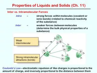
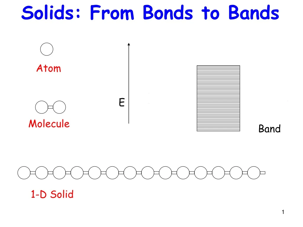
Solids: From Bonds to Bands. Levels. Bond. Molecule. Band. 1-D Solid. Atom. E. Real Materials more complex. Many orbitals per atom Multiple dimensions (3-D). Let us first recap the 1-D bandstructure, so we can see how to generalize it in 3-D. Being systematic helps !!. R = a.

E N D
Solids: From Bonds to Bands Levels Bond Molecule Band 1-D Solid Atom E
Real Materials more complex • Many orbitals per atom • Multiple dimensions (3-D) Let us first recap the 1-D bandstructure, so we can see how to generalize it in 3-D. Being systematic helps !!
R = a R = a K x x x x x x -2p/a 0 2p/a Summary of 1D bandstructure STEP 1: Find period in real space STEP 2: Find k-space periodicity (connecting equivalents points in k-space) K.a = 2p STEP 3: Find BZ by bisecting nearest neighbor connectors. This gives the smallest zone in k-space for a non-repeating band. In this case, it’s between –p/a and p/a. On occasion, this may need you to choose a multiatom or multiorbital basis
-p/a p/a 0 n n-1 n+1 Hk = [Hnn] + [Hn,n+1]eika + [Hn,n-1]e-ika Hn,n-1 Hn,n+1 Hnn b bands x x x x x x . . . . . . . . . . . . Summary of 1D bandstructure STEP 4: Choose N allowed k-points by imposing periodic boundary conditions after N unit cells. For complex solids, we may need to choose specific directions. STEP 5: Identify nearest neighbors and find Fourier transform of H terms over this range for each allowed k. Each [Hnn] has size bxb (b: # basis sets) STEP 6: Find eigenvalues E(k). This gives b bands for each k within the BZ. k= (n/N)K, where n=0,1,2,…,N-1, and K=2p/a
Summary of 1D bandstructure STEP 6: Use this bandstructure E-k to calculate DOS D(E), fit parabolas to extract effective mass m*, etc. These are then used for calculating electronic properties like transmission, I-V, etc.
General prescription in 3-D 1 2 4 0 [H]nm 3 Identify real and k-space lattice vectors Identify Brillouin zone Choose grid points along suitable directions in k-space Find H(k) by summing over nearest neighbor H terms with Fourier phases Find eigenvalues to get E-k, which we then use as needed
Finding real-space periodicity (Lattice vectors)
Simple cubic lattice a = (1,0,0)a b = (0,1,0)a c = (0,0,1)a Lattice Vectors Three primitive vectors are ‘coordinates’ in terms of which all lattice coordinates R can be expressed R = ma + nb + pc (m,n,p: integers)
a = a(0, ½, ½) b = a(½, 0, ½) c = a(½, ½, 0) Face-centered cube 6 face center atoms shared by 2 cubes each, 8 corners shared by 8 cubes each, giving a total of 8 x 1/8 + 6 x 1/2 = 4 atoms/cell
a = a(½, ½, ½ ) b = a(-½,-½, ½ ) c = a(½,-½,-½ ) Body-centered cube 8x1/8 corner atom + 1 center atom gives 2 atoms per cell
Finding k-space periodicity (Reciprocal Lattice vectors)
R = ma + nb + pc (m,n,p: integers) Not to be confused with coordinate r of electron which is spread out everywhere K = MK1 + NK2 + PK3 (M,N,P: integers) Need to find reciprocal basis sets K1, K2, K3 such that reciprocal lattice coordinates can be written as First let’s Fourier transform the lattice Coordinates of periodic lattice (ie atoms)
R = ma + nb + pc (m,n,p: integers) To create analogy with 1-D, want K1 to be orthogonal to b and c, and have a 2p overlap with a so that exp(iK.R) = 1 K1 = 2p(b x c)/[a. (b x c)] K = MK1 + NK2 + PK3 (M,N,P: integers) What are lattice vectors in reciprocal space? Pts in k-space spaced by integer # of K’s represent same electronic state
Choosing k values M, N, P unit cells along Reciprocal lattice vectors k = (m/M)K1 + (n/N)K2 + (p/P)K3 m=0,1,2,…(M-1) n=0,1,2,…(N-1) p=0,1,2,…(P-1)
K2 K1 A simple 2-D Example b a In 3-D Reciprocal lattice of BCC FCC !!
Now to find smallest unit cell volume in k-space (Brillouin zone) First let’s do the same in real space (Wigner-Seitz cell)
How to pick a “Primitive” Unit cell? Two atoms in cell. Want to take a smaller ‘primitive’ cell which only contains 1 atom Many ways to do this
How to pick a “Primitive” Unit cell? The special ‘Wigner- Seitz Cell’ is the one that preserves the translational/rotational symmetry of the lattice • Join nearest neighbors • Bisect these lines • Join the bisectors
3-D Wigner-Seitz Cell • Complicated, but it’s the smallest volume in real-space with 1 atom in it • Join nearest neighbors with center atom, draw bisecting planes, and identify volume enclosed by them • To get smallest range of unique k-values for E-k, just need to Fourier transform this! • ie,Wigner-Seitz in Fourier space Brillouin Zone
Choose specific directions within the BZ to plot E-k along
E K along X direction (100, 010, 001 etc) Real Materials more complex • Many orbitals per atom (many bands) • Multiple dimensions (3-D) • Let us look at bands for silicon
E L valley along (111) Real Materials more complex • Many orbitals per atom (many bands) • Multiple dimensions (3-D) • Let us look at bands for silicon L G X
Real Materials more complex • Many orbitals per atom (many bands) • Multiple dimensions (3-D) • Let us look at bands for silicon E E L G X Combine these into 1 figure
Now that we’ve identified k directions,let’s choose a grid of k points, and find the E-k
S S (bx1) m[H]nm{fm} = E{fm} m[H]nmeik.(dm-dn) Try {fm} = {f0}eik.dm (Bloch’s Theorem) Remember these are coeffs of f in atomic {um} basis Solution E{f0} = [h(k)]{f0} where h(k) = n: any unit cell atom, m: all its nearest neighbors Eigenvalues of h(k) E(k) (bandstructure) General prescriptions 1 b basis sets per atom Equation for mth atom 2 4 0 [H]nm 3
Some important materials Cu: Metal
Some important materials GaAs: Direct Bandgap
E DOS Some important materials Si: Indirect Bandgap
3 3 2 2 1 1 2 FCC lattices interpenetrating, displaced by ¼ the body diag Where are the dimers?? Along body diagonal (111 dirn), atoms unequally placed But along x-axis (100) atoms equally placed
With s orbitals alone, dimerization takes care of gap in (111) direction, not (100) • To get gap in (100), need s and p orbitals, since projection of p orbitals unequal • To get indirect bandgap, need s, p, s* orbitals
Approximations to bandstructure Properties important near band tops/bottoms Described through Constant Energy ellipsoids
hh lh Approximations to bandstructure In contrast, valence bands are more warped and are hard to write as parabolas. One uses 6 band k.p for instance..