Download
1 / 13
130 likes | 248 Views
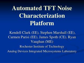
Automated TFT Noise Characterization Platform. Kendell Clark (EE), Stephen Marshall (EE), Carmen Parisi (EE), James Spoth (CE), Ryan Vaughan (ME) Rochester Institute of Technology Analog Devices Integrated Microsystems Laboratory. Project Overview.

E N D
Automated TFT Noise Characterization Platform Kendell Clark (EE), Stephen Marshall (EE), Carmen Parisi (EE), James Spoth (CE), Ryan Vaughan (ME) Rochester Institute of Technology Analog Devices Integrated Microsystems Laboratory
Project Overview • Design & build an automated low noise measurement environment for the purpose of characterizing on wafer devices, specifically monocrystalline silicon TFTs on glass. • Aimed at research groups without the budget to purchase commercially available solutions which can retail at over 1 million dollars. • System should provide a streamlined measurement process which reduces measurement time and complexity.
Project Specifications • Mechanical • Construct an RF/EMI shielded container which fits over existing probe station (Cascade Microtech M150) • Shielded container must not interfere with the normal operation of the probe station. • Must allow probe station microscope to view wafer while in place. • Electrical – Digital Circuitry & Software • Interface custom bias circuitry to lab PC. • Control DUT bias settings, signal amplifiers, and lab measurement equipment. • NO clocks or oscillators allowed in the shielded container.
Project Specifications • Electrical – Analog Bias Circuitry • Allow user to set DUT bias points based off of the device’s I-V curves. • Provide the low level noise signals with adequate amplification so they can be measured by lab equipment. • Noise floor must be as low as possible to ensure accurate noise measurements of the DUT.
Project Specifications • Electrical – Analog Bias Circuitry • Allow user to set DUT bias points based off of the device’s I-V curves. • Provide the low level noise signals with adequate amplification so they can be measured by lab equipment. • Noise floor must be as low as possible to ensure accurate noise measurements of the DUT.
Analog Circuitry – Voltage Bias Circuitry • Control Voltage comes from a DAC located on the PCB. • RFilter & C form a LPF with corner frequency of 1mHz. • >60dB attenuation of noise in the measurement frequency range, 1Hz to 100kHz • RCharge allows for capacitor to reach desired voltage levels quickly.
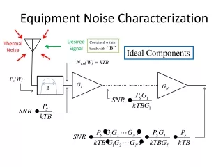
Resistor-Based Current Bias Generation • Uses battery and resistor, or op-amp biasing scheme to produce a fixed voltage across a resistor • Fundamentally limited in noise performance • Resistor thermal noise floor of RD Image: Kwok K. Hung, et. Al. A Physics Based MOSFET Noise Model for Circuit Simulators. IEEE Trans. On Electron Devices. Vol. 37. May 1990.
Analog Circuitry – Current Bias Circuitry • Uses a JFET-based current source • Permits isolation of resistors from output current • Allows resistors to be filtered without attenuating noise at higher frequencies • Circuit topology offers output impedance enhanced by amplifier gain
Analog Circuitry – Current Bias Circuitry Equivalent Noise Model • Use superposition to find contribution of each noise source to output noise current • Choose Cs to attenuate all noise sources appropriately • Assuming large Cs, in1, vn1, inr are made negligible • Amplifier with low vn2 was chosen • JFETs have naturally low in,ch System achieves total output noise current on the order of 100 pA/√Hz
References • [1] Johns, David A. and Ken Martin. Analog Integrated Circuit Design. John Wiley and Sons. 1997. • [2] Stanford Research Systems. Model SR570 – Low Noise Current Preamplifer. SRS, Inc. 1997. • [3] Kwok K. Hung, et. Al. A Physics Based MOSFET Noise Model for Circuit Simulators. IEEE Trans. On Electron Devices. Vol. 37. May 1990. • Expanded list available at booth
Acknowledgements • Dr. Robert J. Bowman, Faculty Advisor and Principal Investigator • Professor George Slack, Faculty Mentor and Guide