Download
1 / 26
260 likes | 407 Views
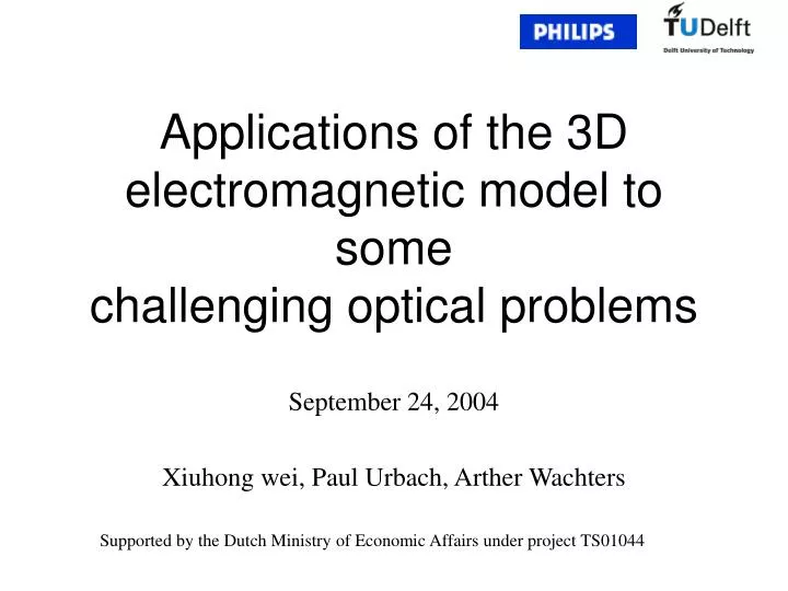
Applications of the 3D electromagnetic model to some challenging optical problems. September 24, 2004 Xiuhong wei, Paul Urbach, Arther Wachters. Supported by the Dutch Ministry of Economic Affairs under project TS01044. Configurations 2D or 3D

E N D
Applications of the 3D electromagnetic model to somechallenging optical problems September 24, 2004 Xiuhong wei, Paul Urbach, Arther Wachters Supported by the Dutch Ministry of Economic Affairs under project TS01044
Configurations • 2D or 3D • Non-periodic structure (Isolated pit in multilayer) • Periodic in one direction (row of pits) • Periodic in two directions (bi-gratings) • Periodic in three directions (3D crystals) • Source • Unrestricted incident field (plane wave, focused spot) • Imposed current density
Materials • Linear. • In general anisotropic, (absorbing) dielectrics and/or conductors: • Magnetic anisotropic materials (for completeness): • Materials could be inhomogeneous:
Mathematical Model • Given field: incident field imposed current • Total field: • Maxwell equations’ are equivalent to Vector Helmholtz Equation: • Scattered field: • The scattered field satisfies the Sommerfeld radiation condition.
Variational formulation • E=E0+Es
iz k j l i • Calculate E0 in Multilayer • S-polarization, i • P-polarization, j • is the source term • Tangential field h(z), e(z) in basis (i,l)
Up and down recursion • Amplitude for planewave • Where are the tangential source term.
Numerical calculation • Construction of Matrix • Matrix property • Complex symmetric • indefinite
Iterative solver • RCM(reversing Cuthill-Mckee) reordering • Precondition • ILUTP(incomplete LU threshold pivoting) • to solve a problem with 300,000 unknows, a fill-in is needed of more than 600, which takes about 25hours on a Hewlett Packard machine (CPU = 107 FLOPS/sec).. • Compare with MRILU(Matries reordering ILU) • More suitable for Finite Difference Method • Complex problems give an extra complication • Krylov subspace method: BICGSTAB (bi-conjugate gradient stabilized algorithm )
Propagation outside of computational domain • The field of Electric Dipole in free space • However we need the field of electric dipole in Multilayer • Calculated by Fourier transformation plane wave expansion • Using recursion as for calculating E0
Stratton-Chu formula Observation point
Results: Near Field Optical Recording • Background • Geometry In the SIL: kx nSIL kx kx nSIL kx Hence, Saptially frequences of the spot are increased , which means the spot became smaller/2 nSIL Cross section
= 405nm • NAeffective= 1.9 • Spotsize /2NAeff=106nm • Grooves(track) Track pitch=226nm Top view
Top view Energy density, wall angle 55, E //groove Energy density , wall angle 55, E groove
Top view Energy density, wall angle 85, E //groove Energy density , wall angle 85, E groove
Cross section xz-plane Energy density, wall angle 55, E//groove Energy density , wall angle 55, E groove
Cross section yz-plane Energy density, wall angle 55, E //groove Energy density , wall angle 55, E groove
Incoherent Light source Condenser Mask Aperture stop Projection lens Photoresist wafer • Lithography • Background • Geometry
260nm 720nm 100nm 340nm • Material: Crome • = 193nm • High NA lithography • nCr=0.86 + 1.65 I • Perpendicular incident planewave
Top view Square mask, E Serif mask, E
Top view Square mask, E Square mask, E
Top view Square mask, finite conduct, E Square mask, Perfect conduct, E
Cross section yz-plane Square mask, finite conduct, E Square mask, Perfect conduct, E
Far field Square mask, E Square mask, E
acknowledge • Our cluster in Philips, Paul Urbach, Arthur wachters, Jan Veerman • Delft mathematical department, Kees Vuik, Kees Oosterlee, Yogi Erlangga, Mari Berglund • Shell staffs, Ren´e-Edouard Plessix, Wim Mulder