Download
1 / 1
10 likes | 117 Views
Logic Gates using Magnetic Dots By: Madhav Rao (Master Student) Advisors: Dr. John C Lusth, Dr. Susan Burkett Department of Computer Engineering and Electrical Engineering, Dr. John Shultz, Morgan Ware, Department of Physics University of Arkansas, Fayetteville. Process Flow.

E N D
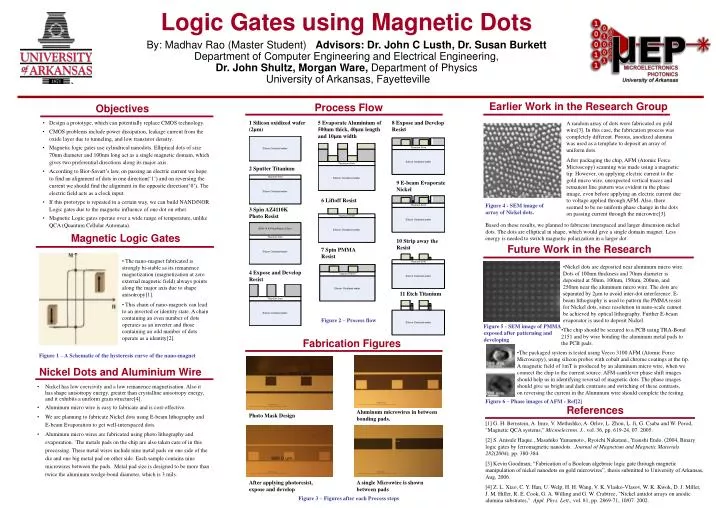
Logic Gates using Magnetic Dots By: Madhav Rao (Master Student) Advisors: Dr. John C Lusth, Dr. Susan Burkett Department of Computer Engineering and Electrical Engineering, Dr. John Shultz, Morgan Ware, Department of Physics University of Arkansas, Fayetteville Process Flow Earlier Work in the Research Group Objectives • Design a prototype, which can potentially replace CMOS technology. • CMOS problems include power dissipation, leakage current from the oxide layer due to tunneling, and low transistor density. • Magnetic logic gates use cylindrical nanodots. Elliptical dots of size 70nm diameter and 100nm long act as a single magnetic domain, which gives two preferential directions along its major axis. • According to Biot-Savart’s law, on passing an electric current we hope to find an alignment of dots in one direction(‘1’) and on reversing the current we should find the alignment in the opposite direction(‘0’). The electric field acts as a clock input. • If this prototype is repeated in a certain way, we can build NAND/NOR Logic gates due to the magnetic influence of one dot on other. • Magnetic Logic gates operate over a wide range of temperature, unlike QCA (Quantum Cellular Automata). 1 Silicon oxidized wafer (2µm) 5 Evaporate Aluminium of 500nm thick, 40µm length and 10µm width 8 Expose and Develop Resist A random array of dots were fabricated on gold wire[3]. In this case, the fabrication process was completely different. Porous, anodized alumina was used as a template to deposit an array of uniform dots. After packaging the chip, AFM (Atomic Force Microscopy) scanning was made using a magnetic tip. However, on applying electric current to the gold micro wire, unexpected vertical traces and remanent line pattern was evident in the phase image, even before applying an electric current due to voltage applied through AFM. Also, there seemed to be no uniform phase change in the dots on passing current through the microwire[3]. 2 Sputter Titanium 9 E-beam Evaporate Nickel 6 Liftoff Resist Figure 4 - SEM image of array of Nickel dots. 3 Spin AZ4110K Photo Resist Based on these results, we planned to fabricate interspaced and larger dimension nickel dots. The dots are elliptical in shape, which would give a single domain magnet. Less energy is needed to switch magnetic polarization in a larger dot. Magnetic Logic Gates 10 Strip away the Resist Future Work in the Research 7 Spin PMMA Resist • The nano-magnet fabricated is strongly bi-stable as its remanence magnetization (magnetization at zero external magnetic field) always points along the major axis due to shape anisotropy[1]. • This chain of nano-magnets can lead to an inverted or identity state. A chain containing an even number of dots operates as an inverter and those containing an odd number of dots operate as a identity[2]. • Nickel dots are deposited near aluminum micro wire. Dots of 100nm thickness and 70nm diameter is deposited at 50nm, 100nm, 150nm, 200nm, and 250nm near the aluminum micro wire. The dots are separated by 2μm to avoid inter-dot interference. E-beam lithography is used to pattern the PMMA resist for Nickel dots, since resolution in nano-scale cannot be achieved by optical lithography. Further E-beam evaporator is used to deposit Nickel. 4 Expose and Develop Resist 11 Etch Titanium Figure 2 – Process flow Figure 5 - SEM image of PMMA exposed after patterning and developing • The chip should be secured to a PCB using TRA-Bond 2151 and by wire bonding the aluminum metal pads to the PCB pads. Fabrication Figures • The packaged system is tested using Veeco 3100 AFM (Atomic Force Microscopy), using silicon probes with cobalt and chrome coatings at the tip. A magnetic field of 1mT is produced by an aluminum micro wire, when we connect the chip to the current source. AFM cantilever phase shift images should help us in identifying reversal of magnetic dots. The phase images should give us bright and dark contrasts and switching of these contrasts, on reversing the current in the Aluminum wire should complete the testing. Figure 1 – A Schematic of the hysteresis curve of the nano-magnet Nickel Dots and Aluminium Wire • Nickel has low coercivity and a low remanence magnetisation. Also it has shape anisotropy energy, greater than crystalline anisotropy energy, and it exhibits a uniform grain structure[4]. • Aluminum micro wire is easy to fabricate and is cost-effective. • We are planning to fabricate Nickel dots using E-beam lithography and E-beam Evaporation to get well-interspaced dots. • Aluminum micro wires are fabricated using photo lithography and evaporation. The metals pads on the chip are also taken care of in this processing. These metal wires include nine metal pads on one side of the die and one big metal pad on other side. Each sample contains nine microwires between the pads. Metal pad size is designed to be more than twice the aluminum wedge-bond diameter, which is 3 mils. Figure 6 – Phase images of AFM - Ref[2] References Aluminum microwires in between bonding pads. Photo Mask Design [1] G. H. Bernstein, A. Imre, V. Metlushko, A. Orlov, L. Zhou, L. Ji, G. Csaba and W. Porod, "Magnetic QCA systems," Microelectron. J., vol. 36, pp. 619-24, 07. 2005. [2] S. Anisule Haque., Masahiko Yamamoto., Ryoichi Nakatani., Yasushi Endo. (2004, Binary logic gates by ferromagnetic nanodots. Journal of Magnetism and Magnetic Materials 282(2004), pp. 380-384. [3] Kevin Goodman, “Fabrication of a Boolean algebraic logic gate through magnetic manipulation of nickel nanodots on gold microwires”, thesis submitted to University of Arkansas, Aug, 2006. [4] Z. L. Xiao, C. Y. Han, U. Welp, H. H. Wang, V. K. Vlasko-Vlasov, W. K. Kwok, D. J. Miller, J. M. Hiller, R. E. Cook, G. A. Willing and G. W. Crabtree, "Nickel antidot arrays on anodic alumina substrates," Appl. Phys. Lett., vol. 81, pp. 2869-71, 10/07. 2002. After applying photoresist, expose and develop A single Microwire is shown between pads Figure 3 – Figures after each Process steps