Download
1 / 1
10 likes | 97 Views
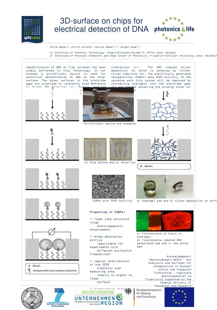
100nm. 3D-surface on chips for electrical detection of DNA. Antje Beyer 1 , Ulrich Arnold 1 , Karina Weber 1,2 , Jürgen Popp 1,2. 1) Institute of Photonic Technology, Albert-Einstein-Straße 9, 07745 Jena, Germany

E N D
100nm 3D-surface on chips for electrical detection of DNA Antje Beyer1, Ulrich Arnold1, Karina Weber1,2, Jürgen Popp1,2 1) Institute of Photonic Technology, Albert-Einstein-Straße 9, 07745 Jena, Germany 2) Institute of Physical Chemistry and Abbe Center of Photonics, Friedrich-Schiller University Jena, Helmholtzweg 4, 07743 Jena, Germany Immobilization of DNA on flat surfaces has been widely performed in Chip Technology. In our studies a microfluidic device is used for electrical determination of DNA on the Chip-surface. The glass surfaces in the electrode gaps are silanized to covalently bind NH2-grous of primer DNA molecules (a). Biotin- labelled target -DNA is hybridized to it (b) and horseradish- peroxidase (HRP) bound via Streptavidin- Biotin- interaction (c). The HRP induces silver deposition (d) which is enhanced by further silver reduction (e). The electrically generated nanoparticles (EGNPs) show SERS activity. In the upcoming work this system will be improved by introducing hydrogels into the electrode gaps (f) and thereby advancing the binding sites for DNA from 2D- to 3D-surfaces (g). f) a) Microfluidic device and examples of Chips a) b) b) g) a) Chip before and b) after silver-deposition c) a) b) d) EGNPs with SERS activity a) Hydrogel pad and b) silver deposition on surface • Properties of EGNPs: • flake like structure (high electromagnetic enhancement) • broad absorption profile (applicable for experiments with different excitation frequencies) • regular distribution of the SERS intensity over measuring area (nearly no signal on clean surface) • quantitative analysis possible a) b) c) a) Fluorescence of Eosin in hydrogel, b) fluorescence labeled DNA penetrated 1mm and c) the whole pad e) Acknowledgment: “Wachstumskern BASIS – Bio Analytics and Surfaces for Integrations in System” within the framework “Innovative – regionale Wachstumskerne” is financially supported by the Federal Ministry of Education and Research (BMBF) Germany.