Download
1 / 2
20 likes | 201 Views
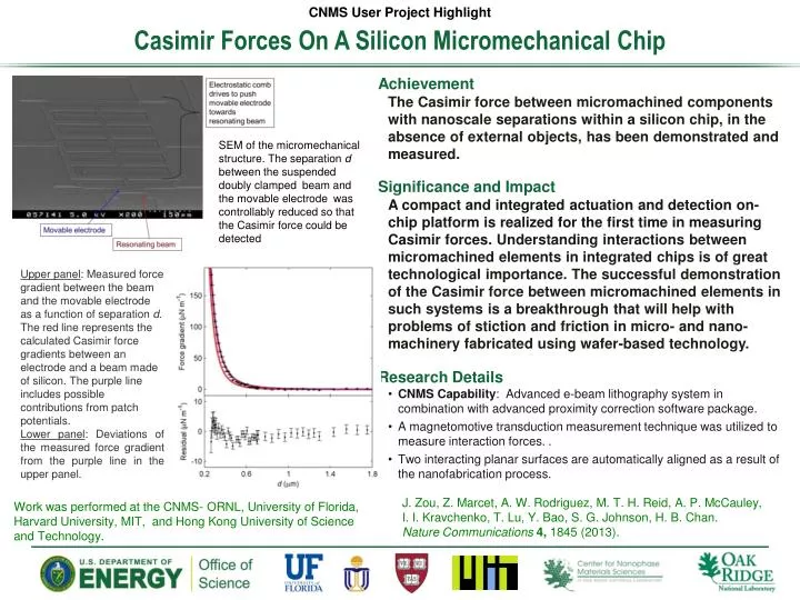
CNMS User Project Highlight. Casimir Forces On A Silicon Micromechanical Chip . Achievement The Casimir force between micromachined components with nanoscale separations within a silicon chip, in the absence of external objects, has been demonstrated and measured. .

E N D
CNMS User Project Highlight Casimir Forces On A Silicon Micromechanical Chip Achievement The Casimir force between micromachined components with nanoscale separations within a silicon chip, in the absence of external objects, has been demonstrated and measured. SEM of the micromechanical structure. The separation d between the suspended doubly clamped beam and the movable electrode was controllably reduced so that the Casimir force could be detected Significance and Impact A compact and integrated actuation and detection on-chip platform is realized for the first time in measuring Casimir forces. Understanding interactions between micromachined elements in integrated chips is of great technological importance. The successful demonstration of the Casimir force between micromachined elements in such systems is a breakthrough that will help with problems of stiction and friction in micro- and nano-machinery fabricated using wafer-based technology. Upper panel: Measured force gradient between the beam and the movable electrode as a function of separation d. The red line represents the calculated Casimir force gradients between an electrode and a beam made of silicon. The purple line includes possible contributions from patch potentials. Lower panel: Deviations of the measured force gradient from the purple line in the upper panel. • Research Details • CNMS Capability: Advanced e-beam lithography system in combination with advanced proximity correction software package. • A magnetomotivetransduction measurement technique was utilized to measure interaction forces. . • Two interacting planar surfaces are automatically aligned as a result of the nanofabrication process. J. Zou, Z. Marcet, A. W. Rodriguez, M. T. H. Reid, A. P. McCauley, I. I. Kravchenko, T. Lu, Y. Bao, S. G. Johnson, H. B. Chan. Nature Communications4, 1845 (2013). Work was performed at the CNMS- ORNL, University of Florida, Harvard University, MIT, and Hong Kong University of Science and Technology.
CNMS User Project Highlight Measuring the attractive force between parallel, uncharged, conducting plates at the nanometer scale Achievement The attractive force between micrometer-sized mechanical components with nanoscale separations, called the Casimir effect, within a silicon chip has been demonstrated and measured in the absence of external objects. Significance and Impact A compact and integrated actuation and detection platform on a single chip is realized for the first time for Casimir force measurement. The successful demonstration of the Casimir force between microscopic elements in such systems is a breakthrough that will help with problems of stiction, where microscale components stick together, and friction in micro- and nano-machinery fabricated using wafer-based technology. A simplified schematic for the Casimir force measurement containing beam, moveable electrode and comb actuator with electrical connections. The separation ‘d’between the suspended doubly clamped beam and the movable electrode was controllably reduced so that the Casimir force could be detected. The measured (black line) and calculated (red line) Casimir force gradient between the beam and the movable electrode as a function of separation d. • Research Details • Fabrication processes used in the semiconductor industry was used to fabricate the compact and integrated platform. Advanced lithography techniques using electron beams were able to precisely place and align two interacting planar surfaces with a high degree of parallelism for the force measurement. Work was performed at the CNMS- ORNL, University of Florida, Harvard University, MIT, and Hong Kong University of Science and Technology J. Zou, Z. Marcet, A. W. Rodriguez, M. T. H. Reid, A. P. McCauley, I. I. Kravchenko, T. Lu, Y. Bao, S. G. Johnson, H. B. Chan. Nature Communications4, 1845 (2013).