Download
1 / 1
20 likes | 232 Views
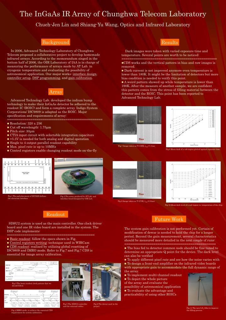
Raw. Raw. CDS. CDS. Bias. Bias. The InGaAs IR Array of Chunghwa Telecom Laboratory. Chueh-Jen Lin and Shiang-Yu Wang, Optics and Infrared Laboratory. Background. Results.

E N D
Raw Raw CDS CDS Bias Bias The InGaAs IR Array of Chunghwa Telecom Laboratory Chueh-Jen Lin and Shiang-Yu Wang, Optics and Infrared Laboratory Background Results In 2006, Advanced Technology Laboratory of Chunghwa Telecom proposed a collaborative project to develop homemade infrared arrays. According to the memorandum singed in the bottom half of 2006, the OIR Laboratory of IAA is in charge of measuring the performance of arrays made by AT Lab. in cryogenic temperature and evaluating the possibility of astronomical application. Our major works: interface design, controller setup, DSP programming, and gain calibration. • Dark images were taken with varied exposure time and temperature. Several points are worth to be noticed: • ================================================= • CDS works and the vertical pattern in bias and raw images is removed. • Dark current is not improved anymore even temperature is lower than 180K. It might be the limitation of detectors but more bias condition is needed to verify this point. • A weird pattern showed up while temperature is lower than 190K. After the measure of another sample, we are confident this pattern comes from the stress of filling material between the detector and the ROIC. This point has been reported to Advanced Technology Lab. Array • Advanced Technology Lab. developed the indium bump technology to make their InGaAs detector be adhered to the readout IC (ROIC) and form a complete array. Indigo System Corporations’ ISC9809 is adapted as the ROIC. Major specification and requirements of array: • ================================================= • Resolution: 320 x 256 • Cut off wavelength: 1.75μm • Pitch size: 30μm • CTIA input circuit with selectable integration capacitors • +5.5V is needed for both analog and digital operation • Single to 4 output parallel readout capability • Max. pixel rate is up to 10MHz • Control registers enable changing readout mode on-the-fly Fig.7 Image taken as T=180K, texp=7.11sec Fig.9 Mean dark of a sub-region plotted against exposure time. Fig.1 The pad placement of ISC9809 defines the electronic interface. Fig.2 The array produced by AT Lab. and interface board designed by OIR Lab. Fig.8 Image taken as T=270K, texp=0.84sec Fig.10 Mean dark level of a sub-region vs. temperature of the chip. Readout Future Work • SDSU2 system is used as the main controller. One clock driver board and one IR video board are installed in the system. The DSP code implements: • ============================================= • Basic readout: follow the specs shown in Fig. • Control registers writing: technique used in WIRCam • CDS readout: realized by utilizing global resetting of ISC9809 and IMRO mode. Refer to Fig.? and Fig.? CDS is essential for image array calibration. • The system gain calibration is not performed yet. Certain of modification of dewar is needed to hold the chip for a longer period. Beyond the gain measurement, several characteristics should be measured more detailed in the next couple of runs: • =============================================== • The bias fed to detector common node should be fine tuned to determine an appropriate Q point for the device. The dark level can also be verified • To apply different pixel rate and see how the noise varies with • To design a front-end amplifier on the infrared video boards with appropriate gain to accommodate the full dynamic range of the array. • To implement multi-channel readout • To depict the whole picture of the array and evaluate the possibility of astronomical application • To evaluate the advantage and practicability of using other ROICs Fig.3 The basic readout clock pattern that we should follow. Fig.5 The SDSU2 controller and the external cables. Fig.6 The dewar used in the project. Fig.11 The new LN2 filler to improve the filling process. Fig.4 IMRO mode, to achieve the essential CDS requirement for system calibration.