Download
1 / 7
80 likes | 1.87k Views
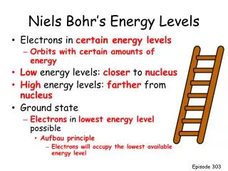
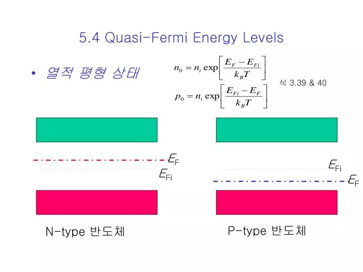
E F E Fi E Fi E F P-type 반도체 N-type 반도체 5.4 Quasi-Fermi Energy Levels 식 3.39 & 40 열적 평형 상태 E F E Fi N-type 반도체 초과 운반자가 존재하면 : 열적 평형 상태가 아님 Fermi 에너지가 정의되지 않음 Quasi -Fermi 에너지를 정의 E Fn E Fp 예제 5.5 Quasi-Fermi 에너지를 구하기 Quasi-Fermi 에너지 개념 : p-n Junction 에서 사용

E N D
EF EFi EFi EF P-type 반도체 N-type 반도체 5.4 Quasi-Fermi Energy Levels 식 3.39 & 40 • 열적 평형 상태
EF EFi N-type 반도체 • 초과 운반자가 존재하면: 열적 평형 상태가 아님 Fermi 에너지가 정의되지 않음 Quasi-Fermi 에너지를 정의 EFn EFp 예제 5.5 Quasi-Fermi 에너지를 구하기 Quasi-Fermi 에너지 개념: p-n Junction 에서 사용
5.5 Excess Carrier Lifetime • 만약 반도체가 perfect하다면: Forbidden band-gap안에 존재 가능한 에너지 상태가 없음 • 실제의 경우: Defect등으로 forbidden band-gap 사이에 Defect State가 존재 가능 • 이러한 State가 lifetime에 큰 영향 • Shockley-Read-Hall Theory 로 mean carrier life time 결정 가능
5.5.1 Shockley-Read-Hall Theory • Allowed 에너지 상태 (Trap): Act as a recombination center. • 전자나 홀을 capture (거의 같은 확률로) • 전자와 홀에 대한 비슷한 capture cross section • S-R-H Theory : Band gap 안에 있는 single trap을 가정해서 recombination rate을 결정
537.622 M154 S-R-H Theory • Four Basic Processes (For Acceptor type 가정) • 전자를 포획 (from conduction band) • 전자를 방출 (to conduction band) • 홀을 포획 (from valance band) • 홀을 방출 (to valance band) (식 5.78) 자세한 유도 과정: John P. McKelvey (pp. 361~368) “Solid State and Semiconductor Physics” Happer & Row,
5.5.2 Limits of Extrinsic Doping & Low Injection n`, p` 의 물리적 의미: 만약 Fermi 에너지가 Et 일 때 conduction(valance) band 에 존재할 전자(홀)의 농도 Low level injection Minority 홀과 관계 For N-type For P-type
5.5.2 Surface Effects • 표면: 많은 Defect, trap 존재 • 표면에서의 Minority carrier lifetime < Bulk • 전체 반도체내에서 일정한 Generation rate 가정하면: • Generation rate = recombination rate • Recombination rate at Surface = at Bulk • Since