Download
1 / 51
520 likes | 673 Views
ELCT 903. Programmable Logic Circuits: Introduction. Dr. Eng. Amr T. Abdel-Hamid. Fall 2010. Course Contents. Introduction to Programmable Logic Devices Number systems and basic arithmetic operations Computer Arithmetic Basic Functions: Addition Multiplication Division

E N D
ELCT 903 Programmable Logic Circuits: Introduction Dr. Eng. Amr T. Abdel-Hamid Fall 2010
Course Contents • Introduction to Programmable Logic Devices • Number systems and basic arithmetic operations • Computer Arithmetic Basic Functions: • Addition • Multiplication • Division • Floating-point arithmetic • Special FP Functions • Pipelining Basics • Test Bench Generation
Course Grading • Exams • Quizzes (10%) 3 Quizzes: best 2 • Midterm (20%) • Final exam (40%) • Assignments (50%) • Project (25%)
Project • Course Project: • Building a Fast Floating Point MIPS Microprocessor • Other topics (after instructor approval) • Mixed Signal Design • IP Protection • More in your master/graduation project topic to publish a paper?
Phase 0: Select your partner (27/9/2010) Submit list of your group members (2-4 per group) Phase 1: . . . . . Phase N: Finael Project Implementation + Report (2 weeks before finals) Project FINAL Non-Negotiable deadline
In time & It is too LATE Policy • In phases 0, & 1: • 5% of project grade penalty per day for being late • In phase 2, to n: • No late presentation is possible. • Honor code • 100% penalty for both copier and copy-giver of Any Report/CODE.
Why PLCs? • Main Design Goal: Construct an implementation with desired functionality. • Key design challenge: Simultaneously optimize numerous design metrics • Design metric: • A measurable feature of a system’s implementation • Optimizing design metrics is a key challenge
Design Challenge • Size: the physical space required by the system • Performance: the execution time or throughput of the system • Power: the amount of power consumed by the system • Energy • What is the difference between power and Energy?
Design Challenge • Time-to-prototype: the time needed to build a working version of the system • Time-to-market: the time required to develop a system to the point that it can be released and sold to customers • Maintainability: the ability to modify the system after its initial release • NRE cost (Non-Recurring Engineering cost): The one-time monetary cost of designing the system • Flexibility: the ability to change the functionality of the system without incurring heavy NRE cost
Time-to Market • Time required to develop a product to the point it can be sold to customers • Market window • Period during which the product would have highest sales • Average time-to-market constraint is about 8 months • Delays can be costly Revenues ($) Time (months)
Delayed Market Entry • Simplified revenue model • Product life = 2W, peak at W • Time of market entry defines a triangle, representing market penetration • Triangle area equals revenue • Loss • The difference between the on-time and delayed triangle areas Peak revenue Peak revenue from delayed entry On-time Market rise Revenues ($) Market fall Delayed D W 2W On-time Delayed entry entry Time
Design Productivity Gap 10,000 100,000 1,000 10,000 100 1000 Logic transistors per chip (in millions) Gap Productivity (K) Trans./Staff-Mo. 10 100 IC capacity 1 10 0.1 1 productivity 0.01 0.1 0.001 0.01 1981 1983 1985 1987 1989 1991 1993 1995 1997 1999 2001 2003 2005 2007 2009 • 1981 leading edge chip required 100 designer months • 10,000 transistors / 100 transistors/month • 2002 leading edge chip requires 30,000 designer months • 150,000,000 / 5000 transistors/month • Designer cost increase from $1M to $300M
The Mythical Man-Month Team 15 60000 16 16 18 50000 19 40000 23 24 30000 Months until completion 20000 43 Individual 10000 0 10 20 30 40 Number of designers • The situation is even worse than the productivity gap indicates • In theory, adding designers to team reduces project completion time • In reality, productivity per designer decreases due to complexities of team management and communication • In the software community, known as “the mythical man-month” (Brooks 1975) • At some point, can actually lengthen project completion time! (“Too many cooks”) • 1M transistors, 1 designer=5000 trans/month • Each additional designer reduces for 100 trans/month • So 2 designers produce 4900 trans/month each
NRE and Unit Cost Metrics Amortizing NRE cost over the units results in an additional $200 per unit • Costs: • Unit cost: the monetary cost of manufacturing each copy of the system, excluding NRE cost • NRE cost (Non-Recurring Engineering cost): the one-time monetary cost of designing the system • total cost = NRE cost + unit cost * # of units • per-product cost = total cost / # of units = (NRE cost / # of units) + unit cost • Example • NRE=$2000, unit=$100 • For 10 units • total cost = $2000 + 10*$100 = $3000 • per-product cost = $2000/10 + $100 = $300
Compare technologies by costs -- best depends on quantity Technology A: NRE=$2,000, unit=$100 Technology B: NRE=$30,000, unit=$30 Technology C: NRE=$100,000, unit=$2 NRE and unit cost metrics • But, must also consider time-to-market
Hardware Design Flow Behavioral Description RTL Implementation Human Human Gate Level Synthesis Logic Synthesis Layout Synthesis Chip Programming Layout (Masks) PLC Manufacturing Product ASIC
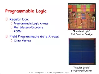
Programmable Logic • Many programmable logic devices are field- programmable, i. e., can be programmed outside of the manufacturing environment • Most programmable logic devices are erasable and reprogrammable. • Allows “updating” a device or correction of errors • Allows reuse the device for a different design - the ultimate in re-usability! • Ideal for course laboratories • Programmable logic devices can be used to prototype design that will be implemented for sale in regular ICs. • Complete Intel Pentium designs were actually prototyped with specialized systems based on large numbers of VLSI programmable devices!
Programmable Logic Circuits • Facts: • It is most economical to produce an IC in large volumes • Many designs required only small volumes of Ics • A programmable logic part can be: • made in large volumes • programmed to implement large numbers of different low-volume designs
Hierarchy of Logic Implementations Standard Logic ASIC Logic Programmable Logic Devices (FPLDs) SemiCustom ICs Full Custom ICs TTL CMOS SPLDs (e.g., PALs) Gate Arrays Cell-Based ICs CPLDs FPGAs
Programming Technologies • Programming technologies are used to: • Control connections • Build lookup tables • Control transistor switching • The technologies • Control connections • Mask programming • Fuse • Antifuse • Single-bit storage element
Programming Technologies • The technologies (continued) • Build lookup tables • Storage elements (as in a memory) • Transistor Switching Control • Stored charge on a floating transistor gate • Erasable • Electrically erasable • Flash (as in Flash Memory) • Storage elements (as in a memory)
Technology Characteristics • Permanent - Cannot be erased and reprogrammed • Mask programming • Fuse • Antifuse • Reprogrammable • Volatile - Programming lost if chip power lost • Single-bit storage element • Non-Volatile • Erasable • Electrically erasable • Flash (as in Flash Memory)
Field- Programmable Logic Devices • Component function is defined by users program. • Logic Cells Fields are interconnected by programming. • Advantages: • Flexible design that changes by reprogramming, ease of design changes • Reduce prototype-product time • Large scale integration (over 100 000 gates) • Reliability increased, low financial risk • Smaller device, low start-up cost 4/13
Programmable Configurations • Read Only Memory (ROM) - a fixed array of AND gates and a programmable array of OR gates • Programmable Array Logic (PAL)Ò - a programmable array of AND gates feeding a fixed array of OR gates. • Programmable Logic Array (PLA) - a programmable array of AND gates feeding a programmable array of OR gates. • Complex Programmable Logic Device (CPLD) /Field- Programmable Gate Array (FPGA) - complex enough to be called “architectures”
ROM • A special device (called a burner), used to put the information, supplies an electrical current to specific cells in the ROM that effectively blows a fuse in them = burning the PROM. From that point on, chip is read-only. • PROM was the first type of user-programmable chip; address lines = logic circuit inputs data lines = logic circuit outputs • PROMs are inefficient architecture for realizing logic circuit: 6/13
Read Only Memory Example X X X D7 D6 X X D5 X D4 D3 A2 A X D2 X X B A1 D1 X A0 D0 C F0 F2 F1 F3 • Example: A 8 X 4 ROM (N = 3 input lines, M= 4 output lines) • The fixed "AND" array is a“decoder” with 3 inputs and 8outputs implementing minterms. • The programmable "OR“array uses a single line torepresent all inputs to anOR gate. An “X” in thearray corresponds to attaching theminterm to the OR • Read Example: For input (A2,A1,A0)= 011, output is (F3,F2,F1,F0 ) = 0011. • What are functions F3, F2 , F1 and F0 in terms of (A2, A1, A0)?
PLA • PLA was the first device developed for implementing • Consist of two levels of logic gates - programmable “wired” AND-plane & OR-plane • Drawbacks: • Expensive to manufacture • Offered somewhat poor speed-performance Note:
Programmable Logic Array Example A B C A B X 1 X X X B C X X 2 X Fuse intact X Fuse blown A C X 3 X X A B X X 4 X X 0 C C B B A A 1 X F 1 F 2 • 3-input, 3-output PLA with 4 product terms • What are the equations for F1 and F2? • Could the PLA implement the functions without the XOR gates?
Programmable Logic Array (PLA) • Compared to a ROM and a PAL, a PLA is the most flexible having a programmable set of ANDs combined with a programmable set of ORs. • Advantages • A PLA can have large N and M permitting implementation of equations that are impractical for a ROM (because of the number of inputs, N, required • A PLA has all of its product terms connectable to all outputs, overcoming the problem of the limited inputs to the PAL Ors • Some PLAs have outputs that can be complemented, adding POS functions
Programmable Logic Array (PLA) • Disadvantages • Often, the product term count limits the application of a PLA. • Two-level multiple-output optimization is required to reduce the number of product terms in an implementation, helping to fit it into a PLA. • Multi-level circuit capability available in PAL not available in PLA. PLA requires external connections to do multi-level circuits.
PAL • Overcame weaknesses of PLA • Single level of programmability - consists of a programmable “wired” AND-plane & fixed OR-gates • Simpler to program and cheaper implementation • Limited numbers of terms in each output
Programmable Array Logic (PAL) • The PAL is the opposite of the ROM, having a programmable set of ANDs combined with fixed ORs. • Disadvantage • ROM guaranteed to implement any M functions of Ninputs. PAL may have too few inputs to the OR gates. • Advantages • For given internal complexity, a PAL can have larger N and M • Some PALs have outputs that can be complemented, adding POS functions • No multilevel circuit implementations in ROM (without external connections from output to input). PAL hasoutputs from OR terms as internal inputs to all ANDterms, making implementation of multi-level circuits easier.
Programmable Array Logic Example AND gates inputs 0 1 2 3 4 5 6 7 8 9 Product 1 X term F 2 1 X X 3 I A 5 1 4 X X X F 5 2 X X 6 X X I B 5 2 7 X X F 8 3 X X 9 X I C 5 3 10 X X F 11 4 X X 12 X I 4 0 1 2 3 4 5 6 7 8 9 • 4-input, 3-output PAL with fixed, 3-input OR terms • What are the equations for F1 through F4? F1 = F2 = F3 = F4 =
RegisterPLA sequential circuits can be realized • Contain flip flops connected to the OR gate outputs • Importance: • Profound effect ondigital hardware design • Basis for more sophisticated architectures 9/13
CPLD possibility to produce devices with higher capacity than SPLDs. • Technology advanced • Structure grows too quickly in size as the number of inputs is increased • Integrating multiple SPLDs onto a single chip - the only feasible way to provide large capacity devices based on SPLD • Programmably connect the SPLD blocks together • Logic capacity up to the equivalent of about 50 typical SPLD devices 10/13
Sequential PLD • Sequential Programmable Logic Device (SPLD)
Complex PLD (CPLD) • CPLD consists multiple SPLD arrays and programmable interconnections. • LAB = SPLD • PIA: Programmable Interconnect Array • LAB & PIA are programmed using software. • CPLD “density” is usually specified in terms of macrocells or LAB. • Altera & Xilinx are the major manufacturers.
Altera CPLDs • Altera produces three lines of CPLDs • EPLD series • MAX series • FLEX series • It also produces a completedesign tool • MAX+PLUS 2 • Quartus II
Xilinx CPLDs • CoolRunner II, XC9500 • XC9500 is similar to MAX 7000, has PAL architecture • CoolRunner II has PLA architecture
CoolRunner II Architecture • FB = LAB • AIM (Advanced Interconnect Matrix) = PIA • 2~32 FBs
FPGA • Provides logic blocks instead of AND or NAND plane • Typical logic blocks is LUT • Volatile devices • Programmable read-only memory (PROM) can be used to make it nonvolatile
FPGA • Difficult extending CPLDs architectures to higher densities - adifferent approach is needed • FPGAs comprise an array of uncommited circuit elements, called logic blocks, and interconnect resources • FPGA configuration is performed through programming by the end user.
LUT as Logic Block 3-input LUT x 1 x 2 0/1 0/1 0/1 0/1 f 0/1 0/1 0/1 0/1 x 3
FPGA concept • Field Programmable Gate Array • Basic elements: • Configurable logic block (CLB) • I/O block • interconnections • CLB is simpler than LAB or FB, but there are many more of them
Configurable Logic Block (CLB) • Many FPGAs are volatile because their LUTs are based on SRAM.