Download
1 / 38
410 likes | 677 Views
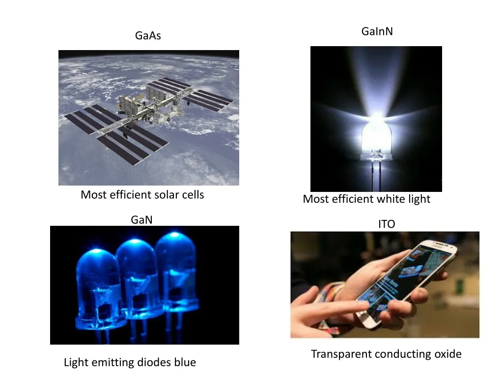
GaInN. GaAs. Most efficient solar cells. Most efficient white light. GaN. ITO. Transparent conducting oxide. Light emitting diodes blue. 1907. The first light emitting diode (LED) made of SiC. Gallium nitride ( GaN ) Aluminium gallium arsenide ( AlGaAs ) Silicon carbide

E N D
GaInN GaAs Most efficient solar cells Most efficient white light GaN ITO Transparent conducting oxide Light emitting diodes blue
1907 The first light emitting diode (LED) made of SiC Gallium nitride (GaN)Aluminium gallium arsenide (AlGaAs) Silicon carbide Gallium phosphide Indium gallium nitride etc Henry Joseph Round To the Editors of Electrical World: SIRS: – During an investigation of the unsymmetrical passage of current through a contact of carborundumand other substances a curious phenomenon was noted. On applying a potential of 10 volts between two points on a crystal of carborundum, the crystal gave out a yellowish light. Only one or two specimens could be found which gave a bright glow on such a low voltage, but with 110 volts a large number could be found to glow. In some crystals only edges gave the light and others gave instead of a yellow light green, orange or blue. In all cases tested the glow appears to come from the negative pole, a bright blue-green spark appearing at the positive pole. In a single crystal, if contact is made near the center with the negative pole, and the positive pole is put in contact at any other place, only one section of the crystal will glow and that same section wherever the positive pole is placed. There seems to be some connection between the above effect and the e.m.f. produced by a junction of carborundum and another conductor when heated by a direct or alternating current; but the connection may be only secondary as an obvious explanation of the e.m.f. effect is the thermoelectric one. The writer would be glad of references to any published account of an investigation of this or any allied phenomena. New York, N. Y. H. J. Round
When electricity is applied , a hole of the p type layer combines with an electron from the n type layer, at the active layer releasing photon whose wavelength is decided by the material at the active layer
2014 Along with Isamu Akasaki and Hiroshi Amano
hc = (1.99 × 10⁻²⁵ joules-m) × (1ev/1.602 × 10-19 joules) = 1.24 × 10⁻⁶ eV-m If the units be in µm (the units for λ): hc = (1.24 × 10⁻⁶eV-m) × (106 µm/ m) = 1.24 eV-µm If in nm hc = 1240 ev- nm We arrive at a commonly used expression which relates the energy and wavelength of a photon, as shown in the following equation: E(eV)=1240λ(nm) λ(μm) = 1240 eV.nm / E (eV) The GaAsbandgap of 1.43 eV, for example, corresponds to a wavelength of approximately 890 nm, which is infrared light (the wavelength for light energy can be determined by dividing the constant 1240 nm-eV by the energy in eV, so 1240 nm-eV/1.4 eV=886 nm). Similarly for gallium nitride GaN 1240/3.45 = 360 nm (close to UV) InNbandgap 0.7 eV GaNbandgap 3.4 eV Range :1770 nm to 360 nm
When electricity is applied , a hole of the p type layer combines with an electron from the n type layer, at the active layer releasing photon whose wavelength is decided by the material at the active layer Ce-YAG Working of a Gallium Indium Nitride LED
White light from LED Spectra of light from white LED
My entry into the field started in April of 1988, when I went to the University of Florida as a visiting researcher. The main purpose of my visit was to learn how to use a MOCVD (Metal Organic Chemical Vapor Deposition) system to growth GaAs crystals on a silicon substrate, as I had no experience in how to use a MOCVD. During my stay there, I worked together with graduate students and they all asked me if I had a Ph.D. I said no. At the time, I only had a Master’s. Next, they asked me if I had published any scientific papers. Again, I said no, I had never published a single paper. Consequently, they treated me as a technician. In the U.S., this meant one has to help the researcher and one’s name would not appear on papers or patents. Gradually, I became very frustrated with this arrangement Shuji Nakamura- NOBEL lecture 2014 One year later, in March of 1989, I came back to Japan. It was my dream to get a Ph.D. degree. In Japan, at the time, it was possible to be awarded a Ph.D. if one published five scientific papers. This type of degree was called a paper degree and one did not need to go to the university to get the degree. It was therefore my ultimate dream to publish at least five papers and get a Ph.D. With this in mind, I noted that the ZnSe field was publishing lots of papers. As I had never published a paper, I had no confidence in publishing a paper. In the GaN field, only very few papers had been published, mainly from Professor Isamu Akasaki and Hiroshi Amano. I was therefore confident that I could publish lots of papers, though had no confidence that I could actually invent the blue LED. My only objective was to get a Ph.D. That’s it.
Gallium – unique properties • Gallium is the only liquid element of the group (m.p.29.7 C). It expands on freezing and unlike mercury, wets glass. • Gallium arsenide, when compared to silicon, has higher saturated electron velocity and high electron mobility which assists transistors of GaAs to work at higher frequencies and with less noise in the circuits. The relatively larger bandgap (1.4 vs 1.1 eV of silicon) leads to insensitivity to overheating of GaAs solar cells. GaAs has therefore been used to make one of the highest-efficiency single-junction solar cells at 28.8% efficiency. • GaAs high operating speed and an ability to operate at low temperatures and under irradiation • Unlike silicon which is a poor emitter of light due to an indirect bandgap (1.1eV), GaAs has a direct and wider band gap (1.4 eV), which translates to absorbing and emitting light efficiently. The wider bandgap also provides resistance to radiation damage and therefore GaAs is an excellent material for outer space electronics and used in high power applications. Unlike silicon, GaAs solar cells have no performance loss when temperature is increased • GaAs is an infrared emitter finding applications in remote controller units.
Gallium nitride, unlike silicon, due to its much wider band gap (3.4 eV) emits brilliant light when a small electric current is passed through it. By varying the band gap, light of any color can be produced. Since indium nitride has a band gap of 0.7 eV, by adding more indium to gallium nitride making InGaN, one can produce different shades of visible light and similarly by adding aluminum one can produce light near the ultra-violet range (AlN band gap (6.01 eV) • Gallium nitride (with Indium gallium nitride as the emitter) based light emitting diodes (LEDs) and laser diodes are already in widespread use as blue LED’s and if one coats a blue LED with a yellow-emitting phosphor (Ce-YAG yttrium aluminum garnet) then bright white light is produced which is now used for white lighting especially replacing regular incandescent and CFL light bulbs. • Being a wide bandgap semiconductor GaN transistors can operate at much higher temperatures and work at much higher voltages than gallium arsenide transistors. They make ideal power amplifiers at microwave frequencies. The band gap is called "direct" if the momentum of electrons and holes is the same in both the conduction band and the valence band; when the band gap is direct, an electron can directly emit a photon. In an "indirect" gap, a photon cannot be emitted because the electron must pass through an intermediate state and transfer momentum to the crystal lattice.
Methods for making thin films of GaAs and GaN: Epitaxial growth techniques The main methods used are Metal organic chemical vapour deposition (MOCVD), Hydride vapour phase epitaxy (HVPE) and Molecular beam epitaxy (MBE). MOCVD uses volatile organogallium compounds such as trimethyl gallium and triethyl gallium to transport gallium atoms to the substrate to be deposited and react with nitrogen sources such as NH3 at a convenient deposition temperature. MOCVD method provides very high quality film, is of intermediate cost and has high growth rate and throughput rate In the HVPE method, the reactor consists of two zones namely the source zone and the growth zone. In the source zone, metallic gallium is reacted with HCl at 860 °C to make GaCl. The gallium monochloride formed is injected into the growth zone using a carrier gas such as hydrogen or ammonia where the substrate to be coated is kept at around 1000 °C and allowed to react with ammonia resulting in the coating of GaN. In the MBE method, elements such as gallium and arsenic, in ultra-pure form, are heated in separate outpouring cells or electron beam evaporators until they start to slowly sublime. The gaseous elements then condense on the wafer, where they react with each other forming the desired semiconductor.
The grown GaN layers using triethylgallium as a precursor exhibited superior electrical and optical properties and a lower carbon impurity concentration. There are two possible reaction mechanisms for the reaction of triethylgallium with ammonia in growing GaN: (1) beta hydride elimination (C2H4+H) and (2) direct desorption of C2H6 (similar to the trimethylgallium growth mechanism).
MOCVD MBE VPE
Can GaN work also as a solar Cell ? Shockley–Queisser limit The limit places maximum solar conversion efficiency around 33.7% assuming a single p-n junction with a band gap of 1.34 eV. That is, of all the power contained in sunlight falling on an ideal solar cell (about 1000 W/m²), only 33.7% of that could ever be turned into electricity (337 W/m²). The most popular solar cell material, silicon, has a less favorable band gap of 1.1 eV, resulting in a maximum theoretical efficiency of about 32%. Crystalline silicon, the most popular solar cell semiconductor, has a bandgap of 1.1 electron volts (eV). The semiconductor chosen for a solar cell has to absorb as much of the solar spectrum as possible, therefore a low band gap is desirable. However, this is counter balanced by the desire to also have as large a built-in voltage as possible which requires a larger band gap. Therefore as a compromise, a band gap between 1.0 and 1.7 eV makes an effective solar semiconductor. In this range, electrons can be freed without creating too much heat.
Wide band gap electronic devices are expected to cut down energy losses. Electronic devices based on them will be able to eliminate up to 90% of the power losses that currently occur during AC-to-DC and DC-to-AC electricity conversion. • They can handle voltages more than 10 times higher than Si-based devices, greatly enhancing performance in high-power applications. They are expected to ensure more reliable and consistent power electronic device operation. • They are suitable for higher-temperature operations:Wide band gap semiconductors are expected to operate at temperatures upto 300°C which is approximately twice the maximum temperature of operation possible for silicon based devices. This tolerance for higher operating temperature results in better overall system reliability, enables smaller and lighter systems and creates opportunities for new applications. • Wide band gap semiconductors are useful for higher frequencies: They operate at frequencies at least 10 times higher than Si-based devices, making possible more compact, less costly product designs and opening up a range of new applications, such as radio frequency (RF) amplifiers. • Wide band gap materials such as GaN or InGaN have greater lighting efficiency: indium gallium nitride devices can emit colors all the way from visible red to ultraviolet, which has made these compounds very attractive. Wide band gap based LEDs produce more than 10 times more light per watt of input energy than comparable incandescent bulbs and extend service life by 30 times or more. The deep ultraviolet LED’s mostly based on GaN have potential applications not only in white lighting (~255 nm) but also in UV based air and water purifiers ( ~ 265 nm) and biomedical sensors (~ 280 nm) worth tens of billions of dollars.
INDIUM • InCl3 is a mild, air and moisture stable Lewis acid which has been found to be useful in acid catalyzed organic reactions. Unlike many other Lewis acids, it has excellent functional group tolerance (such as epoxides, acetals, alkynes and alkenes) and gives better yield and selectivity compared to mild Lewis acids such as ZnCl2. • Indium tin oxide (ITO) is one of the most widely used transparent conducting oxides (TCO). Compared to other TCO’s, its electrical conductivity and optical transparency are quite high, as well as the ease with which it can be deposited as a thin film. Modern day mobile phones, ATM counters and any device using touch screen technology involve use of ITO. It is also used for heating of glass for removing frost formation especially aircraft glass windows.
Indium in organic synthesis Indium metal is air stable and non-toxic with a first ionization potential of 5.8 eV close to Na and Li and is therefore an efficient single electron transfer agent Allyl indium halides are formed without formation of Wurtz type coupling products by mixing indium powder and allyl halides (useful for allylation of carbonyl compounds) . Indium mediated Barbier type allylations are done in water medium Organoindium compounds are tolerant to water and reactions does not need protection of OH or similar protonated functional groups Indium has a tendency to coordinate to heteroatoms especially oxygen of OH or C=O making reactions regio-, stereo and chemo-selective.
70 % of all Indium goes for making Indium Tin Oxide ITO = 90% In2O3, 10% SnO2 When your finger or a suitable object touches the screen, it changes the electrical state at the point of contact. The device then tracks the changes and reacts by completing the tasks the movement of your finger or in the case of multi-touch systems fingers; are requesting.
WHY ITO IS THE MOST SOUGHT AFTER TCO? At a given thickness, it has the highly desired combination of both better electrical conductivity and higher optical transparency compared to any other doped metal oxide. It is easy to be deposited as a thin film (Sputtering), It is more resistance against moisture penetration It has better chemical stability compared to other TCO’s It is easy to be mass produced. Unlike aluminium zinc oxide (AZO) which is less expensive and has also good optical transmission, ITO can be precisely etched into fine patterns. ITO shows almost 90% reflectance of infrared radiation.
1954 ITO resistive capacitive G. Rupprecht reports the semi conducting properties of Indium oxide, In2O3. This was followed by the report by V. A. Williams in 1966 on the potential of tin doped indium oxide (Indium tin oxide, ITO) as a transparent conducting material Applications include liquid crystal, flat panel and plasma displays, touch screen technology of mobile phones and ATM’s, electronic ink, light-emitting diodes, solar cells, antistatic coatings, defrosting aircraft windows and infrared reflecting coatings (oven doors).
By 2017, over a third of the world’s population is projected to own a smartphone an estimated total of almost 2.6 billion smartphone users in the world Approximately 70% of indium has been practically utilized to produce indium tin oxide thin film which is an In–Sn mixed metal oxide consisting of indium oxide (In2O3) and tin oxide (SnO2) at the rough mass ratio of 9:1. The transparent and conducting ITO film is an important material used as the electrode in liquid crystal displays (LCD), which are present in computers, laptops, mobile phones, television sets etc and touch screen devices. Recent metal market prices showed that indium price of 2014 increased by 26% compared with the previous year on the basis of a data analysis at the current indium consumption rate, the indium reserve in the earth’s crust is expected to be exhausted by the year of 2025 .
Resistive versus Capacitive Resistive touchscreens are versatile as they can be operated with a finger, a fingernail, a stylus or any other object. d, the outer later is pushed onto the next layer — the technology senses that pressure is being applied and registers input. Resistivetouchscreens are versatile as they can be operated with a finger, a fingernail, a stylus or any other object. the iPhone was one of the first consumer-focussedsmartphones to use a capacitive touchscreen. This paved the way for today's range of touchscreensmartphones including the wealth of Android smartphones currently available on the market, Capacitive touchscreens work by sensing the conductive properties of an object, usually the skin on your fingertip. A capacitive screen on a mobile phone or smartphone usually has a glass face and doesn't rely on pressure. This makes it more responsive than a resistive screen when it comes to gestures such as swiping and pinching. Capacitive touchscreens can only be touched with a finger, and will not respond to touches with a regular stylus, gloves or most other objects.
Toxicity of thallium and an antidote for thallium poisoning Some of the major toxicological effects of thallium are (a) disruption of potassium-dependent processes, (b) interference with cysteine residues (c) riboflavin sequestration (d) ribosomal inhibition and injury to myelin sheath. Thallium mimics the nutritionally essential element potassium and easily passes through the stomach wall into the blood stream. The body, after a while realizes that it is not potassium and sends it back to the intestines. However, further down the intestines it is again mistaken for potassium and reabsorbed. This cycle need to be broken if thallium is to be removed from the body. Elimination of thallium from the body is slow with a half-life for elimination of 3-30 days. Because of this reason, thallium may act as a cumulative poison. Many complexing agents and chelating ligands were attempted to selectively remove thallium from the system and break the cycle of excretion and absorption without success and thallium poisoning was therefore thought to be incurable. In 1969 the German pharmacist Heydlauf suggested the well known complex, Prussian blue [KFe(Fe(CN)6] as an antidote. The soluble form of Prussian blue exchanges its potassium for thallium to which it is found to bind strongly and gets eliminated from the body.