Download
1 / 23
230 likes | 351 Views
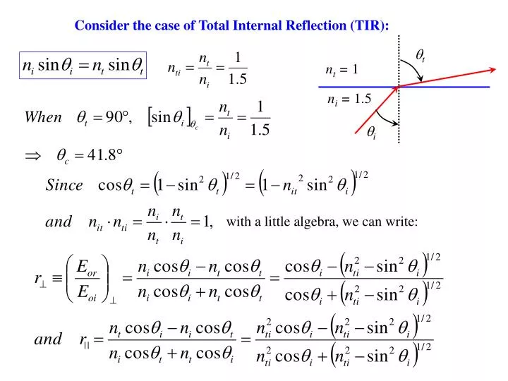
t. n t = 1. n i = 1.5. i. Consider the case of Total Internal Reflection (TIR):. with a little algebra, we can write:. Since sin c = n ti , when i > c , sin i > n ti and r and r || become complex and so r r = r || r || = 1

E N D
t nt = 1 ni = 1.5 i Consider the case of Total Internal Reflection (TIR): with a little algebra, we can write:
Since sin c = nti , when i > c, sin i > nti and r and r|| become complex and so rr = r||r|| = 1 and R = 1 which gives Ir= Ii and It = 0 since R + T = 1. When It = 0, this means that on average the transmitted wave cannot carry energy across the interface boundary in the case of TIR.
Consider now the transmitted E-field: y nt = 1 t x ni = 1.5 i However, when sin i > nti we have
Upon substituting ktx and kty: Only the decaying solution is physically reasonable. y ni=1.5 nt=1 (less dense medium) y = 0 (interface) The E-M wave propagates in the x-direction a Surface or Evanescent Wave. The amplitude decays rapidly in the y-direction, becoming negligible at a distance of only a few wavelengths from the interface.
y x Frustrated Total Internal Reflection (FTIR) Form a sandwich having a glass-air-glass interface: Precision Spacer n= 1.5 n 1 ke n= 1.5 y 3D representation with plane waves near the interface boundary. The amount of energy in the transmitted wave can be controlled by adjusting the spacer thickness y. The phenomenon is therefore analogous to barrier penetration or tunneling of electron waves in quantum mechanics.
(a) Beamsplitters using FTIR (b) Conventional beamsplitter arrangement used to take photographs through a microscope and thus a current application of FTIR. (c) Commercial Beamsplitter cubes commonly found in optics laboratories.
Optical Properties of Metals The presence of an electric field E(r,t) causes a current, owing to the conductivity . Note that which is Ohm’s law at the microscopic level. We can write Maxwell’s equations for an homogeneous, isotropic medium containing charge carriers, such as electrons in a non-magnetic metal: We can easily manipulate the 3rd and 4th equations: Also, we will make use of the vector identity: which is the wave equation in an uncharged conducting medium (i.e. a metal).
Thus, the wave equation for a metal gives a complex dispersion relation k() in which k (~ tilda) here is complex; which leads to a complex index of refraction containing real (nR) and imaginary (nI) parts. Note that the last term in the wave equation is like a damping force and is responsible for absorption. Let’s write the propagating wave as Putting this in a more general form involving a complex exponential:
This is the absorption or attenuation coefficient andd = 1/ is known as the skin or penetration depth. Note that depends on the frequency or wavelength. For materials that are transparent, 1/ >> thickness. For metals, take Cu for example: 1/ 6Å at = 100 nm and 60 Å at = 10,000 nm (IR). This explains the opacity of metals in which the penetration depth is very small and most of the energy is reflected. Imagine the metal as a collection of driven and damped oscillators. Some of the electrons in the metal (valence electrons) are free to move and thus possess no restoring force. Other electrons are bound to the atoms such as in a dielectric material like glass. Remember for an oscillating dipole we derived the classical expression from Newton’s second law:
For the free electrons in a metal, there is no restoring force and o=(ks/me)1/2 0. It is as though electrons are attached by very weak springs. Therefore we have The minus sign indicates that the free electrons oscillate 180 out-of-phase relative to the E-field of the incident light. This oscillation therefore creates light waves that will cancel (interfere destructively with the incident wave) when radiating in the same direction as the incident wave. The result is a rapidly decaying refracted wave, as we have just seen with the attenuation. We can extend the dispersion relation to include both types of electrons (bound and free valence e-’s:
free e-’sbound e-’s Therefore where N is the number of atoms per unit volume; fe is the number of free valence electrons per atom.The second term involving the sum again refers to the bound electrons, as we have seen previously for dielectric materials. If a metal has a particular color (Gold and copper are reddish yellow) it indicates that the atoms of the metal are involved with the selective absorption via bound electrons. We can approximate the above equation further by assuming a negligible contribution from bound e-’s ande 0 for large , i.e. a small dissipation at high frequencies:
Consider the behavior of n() for limiting cases in metals: • < p n2() < 0 and n is complex. Since = 2nI/c, the absorption will be large. • > p n2() > 0 and n is real, absorption is small and we observe a transparency condition. Notably, x-rays (100 Å > > 1Å) will penetrate metals. • Some metals, such as Alkali metals, are transparent even in the ultraviolet. The table below illustrates the calculated plasma frequencies and wavelengths for some Alkali metals.
In general, n is complex and so there is absorption in metals when there is a finite nI. Consider reflection from a metal surface at normal incidence (i = 0). We derived this for a dielectric. For an air-metal interface, take Typical values of nR, nI, and R at =589 nm Notice that the reflectance of Na has a larger R despite its smaller nI.
If the conductivity 0 which gives a dielectric with nI 0, nI << nR, and 0, nR nt • If is large, nI is large and nI >> nR and R1. Ag nI(), nR() Ag is transparent at p 320 nm, at which point nI < nR and R << 1.
Note that Au and Cu exhibit an increasing R in the range 500 nm < < 700 nm, and this provides the reddish-yellow color when the metals are illuminated with white light. Note that the dip in R|| is similar to the case of Brewster’s angle (p) for dielectric interfaces except that R|| > 0 at its minimum, as shown. Phase shifts occur during reflection from a metal surface.Both E|| and E experience phase shifts which are in general between 0 and 180. When i = 90, both E|| and E experience = 180.
Bulk Plasmons and the dispersion relation (k) for a metal We can write the E-M wave equation as Note that (, K) can be complex in general and lead to K which is complex, as we have seen in FTIR. We saw already solutions in which we assumed that the contribution from bound electrons and damping were assumed negligible: Inserting this into the first equation above, we get We assume propagating solutions in which K=k is real.
Light line = ck p No allowed propagating modes k Bulk Plasmon Dispersion Relation Solutions lie above the light line. Typical values for the plasmon energy are …Metals ...Semiconductors (depends on dopant concentration). Surface Plasmon Polaritons Consider an E-M wave that can propagate along the interface between metal and vacuum (i.e. the surface of a metal) or between the metal and a dielectric material. Again, we assume solutions to the E-M wave equation.
z Metal m < 0 0 x Dielectric d > 0 The solutions E(r,t) are of the form: We need to invoke continuity conditions of E|| and (E), along with Gauss’s law:
We can further remove the time dependence in the E-M wave equation by inserting (z > 0) (1) (z < 0) (2) Continuity of Exrequires A = C and for Ez requires mB =dD. Therefore (3) Subtracting Eqs. (1) and (2) and eliminating kzd using Eq. (3) we get
Examine the dielectric constants for both the dielectric and metal layers and determine (kx) for surface plasmons. real d sp 0 p Light line = kx/(do)1/2 -d sp Surface plasmon dispersion is below the light line. 1) For small , m - and kx (do)1/2 = /vd 2) At = sp , m - d (from below) and kx + kx
Light dispersion (a) (b) klight SPP kSPP a nkG nkG klightsin kSPP k Surface Plasmon polaritons (SPPs) in metal nanostructures: the optoelectronic route to nanotechnology, M. Salerno et. al., Opto-electronics Rev. 10(3), 217 (2002). Light is injected from the left, creating surface plasmons (SPs) which propagate to the right. When they reach the end of the gold strip (point S), a transfer of momentum to the SPs causes energy to be transferred back to light, which is subsequently detected with a photon scanning tunneling microscope (PSTM).


![External Website Hosting Business Case [Free Template]](https://cdn4.slideserve.com/7373913/slide1-dt.jpg)