Download
1 / 15
150 likes | 217 Views
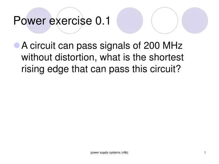
Power exercise 0.1. A circuit can pass signals of 200 MHz without distortion, what is the shortest rising edge that can pass this circuit?. Power exercise 0.1 (answer). A circuit can pass signals of 200 MHz without distortion, what is the shortest rising edge that can pass this circuit? Answer

E N D
Power exercise 0.1 • A circuit can pass signals of 200 MHz without distortion, what is the shortest rising edge that can pass this circuit? power supply systems (v9b)
Power exercise 0.1 (answer) • A circuit can pass signals of 200 MHz without distortion, what is the shortest rising edge that can pass this circuit? • Answer • Fnee=0.5/Tr, so 200MHz=0.5/Tr, Tr=2.5ns. power supply systems (v9b)
Power supply Same dI/dt VL L dI/dt C R Tr Exercise 0.2 5V step 1ns power supply systems (v9b)
Exercise 0.2 ANSWER power supply systems (v9b)
PowerExercise2 • R (internal reference voltage is 2.5V) i.e. • gate_C_out =1 when the input of the gate C amplifier is positive • Else gate_C_out=0 • Now V1=2.8V, R (internal reference voltage is 2.5V, • What is Gate_C_out when • (i) noise N=0? • (ii) noise N=0.5? • (ii) Why there is noise N? power supply systems (v9b)
PowerExercise2(ANS) • R (internal reference voltage is 2.5V) i.e. • gate_C_out =1 when the input of the gate C amplifier is positive • Else gate_C_out=0 • Now V1=2.8V, R (internal reference voltage is 2.5V, • What is Gate_C_out when • (i) noise N=0? Ans: 2.8-0-2.5=0.3 positive, gateC out 1 • (ii) noise N=0.5? Ans:2.8-0.5-2.5=-0.2V neg. so gateC out is 0 (ii) Why there is noise N? ans:ground loop, long wire power supply systems (v9b)
Power Exercise 3Method 1(differential signaling) to reduce ground noise (expensive) by using differential logic gates and transmission lines • Gate C sees V_diff • V0=2.5 (fixed), • When gate 1 is on, V1 =2.5 else V1=0 • A method to remove ground line noise • But very expensive, each bit has 2 lines instead of 1. • Exercise: When gate A is on , N=0.5V , what is Vdiff? • Exercise: When gate A is off , N-0.5V, what is Vdiff? power supply systems (v9b)
Power Exercise 3Method 1(differential signaling) to reduce ground noise (expensive) by using differential logic gates and transmission lines • Gate C sees V_diff • V0=2.5 (fixed), • When gate 1 is on, V1 =2.5 else V1=0 • A method to remove ground line noise • But very expensive, each bit has 2 lines instead of 1. • Exercise: When gate A is on , N=0.5V , what is Vdiff? ANS:5V, N has no effect • Exercise: When gate A is off , N=0.5V, what is Vdiff? ANS:0V, N has no effect power supply systems (v9b)
Power exercise 4 • A hardware system has 500 digital outputs, each output is switching a 10-pF load at 5ns. • The power comes from a perfect voltage source of 5V via a power cable of inductance 200nH. • The maximum allowable supply voltage drop at the system is 0.1V. • The series inductance of each capacitor (for all types) is 5nH. Ignore the inductance of the traces in the system board. State any assumptions you used in the calculations. • Find board level bypass capacitor C2 • Find the number N of elements in the capacitor array and its individual value C3. power supply systems (v9b)
Answer: • Board level bypass capciator(C2)=500uF • Capacitor array totoal=C_total_array=12.5uF • Number o capacyor in the cap. Array(N)=157 • Each element of the cap. array isC3 = 0.079uF. Power Answer 4 • Answer: • Find max. tolerable impedance. • Find the change of current dI=N*C*dv/dt=500*10pF*5/5ns=5A • This dI will cause voltage drop at the power cable and is less than 0.1v, so X=0.1V/5A=0.02ohms • For the by-pass cap. It is effective when the power cable is 0.02ohms, and that is when the frequency is F1, so 2*pi*F1*L_cable=0.02Volts, F1=0.02/(2*pi*200nH)=15.9KHz. • At F1 =15.9KHz, the by-pass cap (c2) should have inductance of 0.02ohms, so 0.02=1/(2*pi*F1*C2), hence C2=1/(2*0.02*pi*15.9K)=500uF • At higher frequency, the cap array takes effect, now it is the problem of the inductance at the legs of the by-pass cap(C2).,so 0.02 Ohms= 2*pi*F2*L_by_pass_cap, F2=0.02ohms/(2*pi*5nH)=636.6KH(to be used later for cap array calculation) • For the cap array-(step1) find N first 2*pi*F3*L_total_array, F3=0.5/Tr=0.5/5ns=100MHz. Since 2*pi*F3*L=X_L or L=X_L/(2*pi*F3), So L_total_array= X_L /(2*pi*100M)=0.2ohms/(2*pi*100M)=0.0318nH. Using N small caps. Each is 5nH, so L_total_array=L_each/N, 0.0318nH =5nH/N, N=157. • For the cap array-(step2) find C_array The cap array should supply current power to the system above F2, so 0.02=1/(2*pi*F2*C_total_array), C_total_array=1/(2*Pi*0.02*636.6K)=12.5uF • So the value (C3) of each element of the cap. array is C3=12.5uF/157= 0.079uF. power supply systems (v9b)
Overall impedance X and Freq. plot Current from board level bypass capacitorC2 Current from Cap. Array C_total_array =N*C3 Current from power supply No current demand here XC2 XC3_array Xpcable XLtot3 XLC2 X 0.1 F1=15.9KHz F3=100MHz F2=636.6KHz power supply systems (v9b)
Power cable with inductance =150nH A large PCB Circuit trace with inductance=35nH Power supply + Ground • Circuit group A: • 100 outputs • each output has a capacitive load of 10pF. • switching time is 10ns Circuit trace with inductance=60nH • Circuit group B • 120 outputs • each output has a capacitive load of 5pF. • switching time is 15ns Power Exercise 5 • A large PCB board contains two circuit areas groups, A and B. The overall power comes from a perfect voltage source of 5Volts. The maximum allowable supply voltage drop anywhere in the board is 0.1Volts. • Given that dI = |C (dV/dt)|, for dI is the change in current, C is the capacitance of the capacitor and dV/dt is the rate of change of the voltage. The board level bypass capacitors for serving both group A and B have a very small series inductance. State any assumptions you used in the calculations. • Three large board level by-pass capacitors are provided, how do you place them? Copy the following diagram to your answer book and insert the bypass capacitors in your diagram. • Calculate the values required? Show your calculation power supply systems (v9b)
Power cable with inductance =150nH A large PCB Circuit trace with inductance=35nH Power supply + Ground • Circuit group A: • 100 outputs • each output has a capacitive load of 10pF. • switching time is 10ns C1 C2 Circuit trace with inductance=60nH • Circuit group B • 120 outputs • each output has a capacitive load of 5pF. • switching time is 15ns C3 Answer 5-c1 • Answer: • Find the overall by-pass cap C1 • I=Na*Ca*dv/dt +Nb*Cb*dv/dt • =100*10pF*5/10ns+120*5pF*5/15ns • =0.5+0.2=0.7A • 3 caps are need, C1, C2, C3. • Voltage drop allowed is 0.1V, so impedance allowed is 0.1V/0.7A=0.143 Ohms. • At freq F1, power cable impedance should be equal to 0.143 Ohms • 2*Pi*F1*150nH=0.143 Ohms. • F1=152 KHz. • C1 will provide an impedance less than 0.143Ohms at F1, • So • 1/(2*pi*F1*C1)=0.143 • C1=7.3uF power supply systems (v9b)
Power cable with inductance =150nH A large PCB Circuit trace with inductance=35nH Power supply + Ground • Circuit group A: • 100 outputs • each output has a capacitive load of 10pF. • switching time is 10ns C1 C2 Circuit trace with inductance=60nH • Circuit group B • 120 outputs • each output has a capacitive load of 5pF. • switching time is 15ns C3 Answer5-c2 • ------------------------- • Find C2 • I=Na*Ca*dv/dt • =100*10pF*5/10ns • =0.5A • Voltage drop allowed is 0.1V, so impedance allowed is 0.1V/0.5A=0.2 Ohms. • At freq F2, power cable impedance should be equal to 0.2 • 2*Pi*F2*35nH=0.2 Ohms. • F2=909KHz. • C2 will provide an impedance less than 0.2 Ohms at F2, • So • 1/(2*pi*F2*C2)= 1/(2*pi*909KHz*C2)=0.2 • C2=0.875uF power supply systems (v9b)
Power cable with inductance =150nH A large PCB Circuit trace with inductance=35nH Power supply + Ground • Circuit group A: • 100 outputs • each output has a capacitive load of 10pF. • switching time is 10ns C1 C2 Circuit trace with inductance=60nH • Circuit group B • 120 outputs • each output has a capacitive load of 5pF. • switching time is 15ns C3 Answer5-c3 • ------------------------- • Find C3 • I=Nb*Cb*dv/dt • =120*5pF*5/15ns • =0.2A • Voltage drop allowed is 0.1V, so impedance allowed is 0.1V/0.2A=0.5 Ohms. • At freq F3, power cable impedance should be equal to 0.5 Ohms. • 2*Pi*F3*60nH=0.5 Ohms. • F3=1.326 MHz. • C3 will provide an impedance less than 0.5 Ohms at F3, • So • 1/(2*pi*F3*C3)= 1/(2*pi*1.326MHz*C3)=0.5 • C3=0.24uF power supply systems (v9b)