Download
1 / 24
550 likes | 2.23k Views
Numericals on semiconductors. Calculate the total number of energy states per unit volume, in silicon, between the lowest level in the conduction band and a level kT above this level, at T = 300 K. The effective mass of the electron in the conduction band is 1.08 times that of a free-electron.

E N D
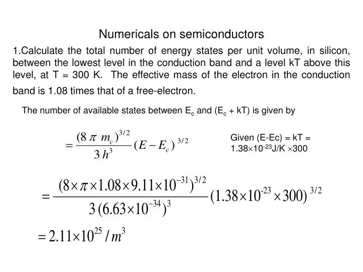
Numericals on semiconductors • Calculate the total number of energy states per unit volume, in silicon, between the lowest level in the conduction band and a level kT above this level, at T = 300 K. The effective mass of the electron in the conduction band is 1.08 times that of a free-electron. The number of available states between Ec and (Ec + kT) is given by Given (E-Ec) = kT = 1.3810-23J/K 300
Numericals on semiconductors 2 Calculate the probability that an energy level (a) kT (b) 3 kT (c) 10 kT above the fermi-level is occupied by an electron. Probability that an energy level E is occupied is given by f(E) = For (E-EF) = kT , f(E) = For (E-EF) = 3kT, f(E) = For (E-EF) = 10kT, f(E) =
Numericals on semiconductors 3 The fermi-level in a semiconductor is 0.35 eV above the valence band. What is the probability of non-occupation of an energy state at the top of the valence band, at (i) 300 K (ii) 400 K ? The probability that an energy state in the valence band is not occupied is (i) T=300K 1-f(E) = = Alternate method: for EF-EV > kT 1- f(E) (ii) T=400K 1-f(E)
Numericals on semiconductors 4 The fermi-level in a semiconductor is 0.35 eV above the valence band. What is the probability of non-occupation of an energy state at a level kT below the top of the valence band, at (i) 300 K (ii) 400 K? The probability that an energy state in the valence band is not occupied is for EF- E> kT (i) T=300K 1 - f(E) = (ii) T=400K 1- f(E) Note (E -EF) is -ve
Numericals on semiconductors 5 For copper at 1000K (a) find the energy at which the probability P(E) that a conduction electron state will be occupied is 90%. (b) For this energy, what is the n(E), the distribution in energy of the available state? (c) for the same energy what is n0( E) the distribution in energy of the occupied sates? The Fermi energy is 7.06eV. The fermi factor f(E) = = 0.90
Numericals on semiconductors contd Density of available state n (E) 5
Numericals on semiconductors The density of occupied states is = (The density of states at an energy E ) ( probability of occupation of the state E) 5contd i.e no (E) = n (E) f(E)
Numericals on semiconductors 6 An intrinsic semiconductor has energy gap of (a) 0.7 eV (b) 0.4 eV. Calculate the probability of occupation of the lowest level in the conduction band at (i) 0C (ii) 50C (iii) 100C. f(E) = a) (i) (ii) (iii)
Numericals on semiconductors 6 An intrinsic semiconductor has energy gap of (a) 0.7 eV (b) 0.4 eV. Calculate the probability of occupation of the lowest level in the conduction band at (i) 0C (ii) 50C (iii) 100C. f(E) = b) (i) (ii) (iii)
Numericals on semiconductors 7 The effective mass of hole and electron in GaAs are respectively 0.48 and 0.067 times the free electron mass. The band gap energy is 1.43 eV. How much above is its fermi-level from the top of the valence band at 300 K? Fermi energy in an Intrinsic semiconductor is Write The fermi level is 0.75eV above the top of the VB
Numericals on semiconductors 8 Pure silicon at 300K has electron and hole density each equal to1.51016 m-3. One of every 1.0 107 atoms is replaced by a phosphorous atom. (a) What charge carrier density will the phosphorous add? Assume that all the donor electrons are in the conduction band. (b) Find the ratio of the charge carrier density in the doped silicon to that for the pure silicon. Given: density of silicon = 2330 kgm-3; Molar mass of silicon = 28.1 g/mol; Avogadro constant NA = 6.02 10 23 mol -3. No of Si atoms per unit vol = Carriers density added by P = Ratio of carrier density in doped Si to pure Si =
Numericals on semiconductors 9 The effective mass of the conduction electron in Si is 0.31 times the free electron mass. Find the conduction electron density at 300 K, assuming that the Fermi level lies exactly at the centre of the energy band gap (= 1.11 eV). Electron concentration in CB is =
Numericals on semiconductors 10 In intrinsic GaAs, the electron and hole mobilities are 0.85 and 0.04 m2 V-1s-1 respectively and the effective masses of electron and hole respectively are 0.068 and 0.50 times the electron mass. The energy band gap is 1.43 eV. Determine the carrier density and conductivity at 300K. Intrinsic carrier concentration is given by ni
Numericals on semiconductors 10 In intrinsic GaAs, the electron and hole mobilities are 0.85 and 0.04 m2 V-1s-1 respectively and the effective masses of electron and hole respectively are 0.068 and 0.50 times the electron mass. The energy band gap is 1.43 eV. Determine the carrier density and conductivity at 300K. Conductivity of a semiconductor is given by mho / m
Numericals on semiconductors 11 A sample of silicon at room temperature has an intrinsic resistivity of 2.5 x 10³ Ω m. The sample is doped with 4 x 10¹⁶ donor atoms/m3 and 1016 acceptor atoms/m3. Find the total current density if an electric field of 400 V/m is applied across the sample. Electron mobility is 0.125 m2/V s. Hole mobility is 0.0475 m2/V.s. Effective doped concentration is
Numericals on semiconductors From charge neutrality equation From law of mass action Solving for p and choosing the right value for p as minority carrier concentration
Numericals on semiconductors Since the minority carrier concentration p < ni Conductivity is given by From Ohm’s law
Numericals on semiconductors 12 A sample of pure Ge has an intrinsic charge carrier density of 2.5 x 10¹⁹/m3 at 300 K. It is doped with donor impurity of 1 in every 106 Ge atoms. (a) What is the resistivity of the doped-Ge? Electron mobility and hole mobilities are 0.38 m2/V.s and 0.18 m2/V.s . Ge-atom density is 4.2 x 1028/m3. (b) If this Ge-bar is 5.0 mm long and 25 x 10–12 m2 in cross-sectional area, what is its resistance? What is the voltage drop across the Ge-bar for a current of 1A? No of doped carriers = Since all the atoms are ionized, total electron density in Ge Nd+ = 4.2 x 10 2 2 /m3
Numericals on semiconductors • From law of mass action Electrical conductivity =
Numericals on semiconductors 12 Contd Resistance Of the Ge bar R = Voltage drop across the Ge bar =
L t Y (-VH) w X (I) Numericals on semicodnuctors 13 A rectangular plate of a semiconductor has dimensions 2.0 cm along y direction, 1.0 mm along z-direction. Hall probes are attached on its two surfaces parallel to x z plane and a magnetic field of 1.0 tesla is applied along z-direction. A current of 3.0 mA is set up along the x direction. Calculate the hall voltage measured by the probes, if the hall coefficient of the material is 3.66 10–4m3/C. Also, calculate the charge carrier concentration. Hall voltage is given by Charge carrier density = Z (B)
Numericals on semiconductors 14 A flat copper ribbon 0.330mm thick carries a steady current 50.0A and is located in a uniform 1.30-T magnetic field directed perpendicular to the plane of the ribbon. If a Hall voltage of 9.60 V is measured across the ribbon. What is the charge density of the free electrons? Charge carrier density n is given by n =
Numericals on semiconductors 15 The conductivity of intrinsic silicon is 4.17 x 10⁻⁵/Ω m and 4.00 x 10⁻⁴ / Ω m, at 0 C and 27 C respectively. Determine the band gap energy of silicon. Intrinsic conductivity =
Numericals on semiconductors • 15 Contd