Download
1 / 20
200 likes | 242 Views
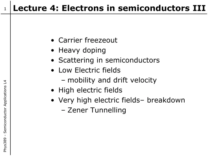
Carrier freezeout Heavy doping Scattering in semiconductors Low Electric fields mobility and drift velocity High electric fields Very high electric fields– breakdown Zener Tunnelling. Lecture 4: Electrons in semiconductors III.

E N D
Carrier freezeout Heavy doping Scattering in semiconductors Low Electric fields mobility and drift velocity High electric fields Very high electric fields– breakdown Zener Tunnelling Lecture 4: Electrons in semiconductors III Phys389 - Semiconductor Applications L4
How do we know that a donor atom electron will occupy an energy level Ed below the conduction band or become a free electron in the conduction band? At low temperature the electrons are confined to the donor atom. The free electron density is zero, we have carrier freezeout. With increasing temperature, the fraction of ionised donors increases until the free carrier density is equal to the donor density. This region is known as the saturation region. With further increase in temperature, the carrier density starts to increase because of the intrinsic carrier density exceeding the donor density. We have the intrinsic region. Carrier Freezeout Phys389 - Semiconductor Applications L4
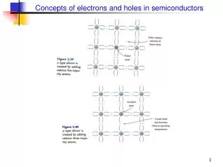
Carrier Freezeout n = total free electrons in conduction band nd= electrons bound to donors p = total free holes in the valence band pa = holes bound to the acceptors Phys389 - Semiconductor Applications L4
The fraction of electrons tied to donor levels in an n-type material with doping density Nd is: The donor ionization energy (Ec-Ed) and temperature determine the fraction of bound electrons. At low temperatures the ratio nd/(n+nd) 1 so that all electrons are bound to donors. A similar result can be produced for p-type material: For electronic devices at room temperature it will be assumed the n=Nd and p=Pa for n and p-type materials respectively Carrier Freezeout Phys389 - Semiconductor Applications L4
A sample of silicon is doped with phosphorus at a doping density of 1016cm-3. What is: The fraction of ionised donors at 300K. The change if the doping density is 1018cm-3 For Si Nd=1016cm-3 (donor BE=45meV) nd is only 0.4% of the total electron concentration and almost all donors are ionised. For a donor level of 1018 Heavy doping and only 71% of dopants are ionised. Carrier Freezeout: Example Phys389 - Semiconductor Applications L4
We have assumed the doping levels are low in our theory so far which means: The bandstructure of the host crystal is not seriously perturbed and the bandedges are still described by simply parabolic bands. The dopants are independent of each other and therefore their potential is a simple Coulombic potential. This is not valid when the spacing of the impurity atoms reaches ~10nm At high doping levels we will get impurity bands. The bandgap will narrow resulting in poor performance for a number of electronic devices Heavily Doped Semiconductors Phys389 - Semiconductor Applications L4
The equation of motion for a free electron is: Quantum mechanics states that in a perfect semiconductor there is no scattering of electrons as they move through the periodic lattice structure. The presence of lattice imperfections will cause electron scattering. If a beam of electrons is incident on a semiconductor, the average time it takes to lose coherence of the initial state values is called the relaxation time (tsc). The average distance between collisions is called the mean free path. Scattering in semiconductors Phys389 - Semiconductor Applications L4
Under thermal equilibrium, the average thermal energy of a conduction electron can be obtained from the theorem of equipartition of energy. 1/2kT units of energy per degree of freedom. The electrons in a semiconductor have three degrees of freedom; they can move about in three dimensional space. The kinetic energy of electrons is hence given by: vth is the average thermal velocity of electrons. At room temperature the thermal velocity is about 107cm/s for Si and GaAs. Scattering in semiconductors Phys389 - Semiconductor Applications L4
Sources of scattering Ionised impurities Due to dopants in the semiconductor Phonons Due to lattice vibrations at finite temperatures result in bandedge variations Alloy Random potential fluctuations in alloy semiconductors (MOSFET) Interface roughness Important in heterostructure devices Chemical impurities Due to unintentional impurities A total scattering rate can be defined: tisc is the scattering time of the electrons due to each individual scattering process. For a typical value of 10-5cm for the mean free path, t(Iisc is about 1ps Phys389 - Semiconductor Applications L4
With the application of an E-field, the electrons move under the external force. A steady state is established in which the electrons have a net drift velocity in the field direction. In the absence of any applied field the electron distribution is given by the Fermi-Dirac distribution. When a field is applied a new distribution which is a function of the scattering rates and field strength is introduced – it is determined by solving the Boltzmann transport equation. The response of electrons to the field can be represented by a velocity-field relationship. E-fields in semiconductors Phys389 - Semiconductor Applications L4
Macroscopic transport properties: Mobility Conductivity Microscopic properties: Scattering rate Relaxation time At low fields the above quantities can be related. Assumptions: The electrons in the semiconductor do not interact with each other the independent electron approximation. Electrons suffer collisions from various scattering sources. tsc describes the mean time between respective collisions. In between collisions electrons move according the equation of motion for a free electron. After a collision the electrons lose all their excess energy Low field response Phys389 - Semiconductor Applications L4
Assuming immediately after a collision the electron velocity is zero and that the electron gains velocity in between collisions for time tsc. The average velocity gain is: vd is the drift velocity. The current density is hence: Recall the mobility (m) defines the proportionality factor between the drift velocity and the applied E field: Low field response Phys389 - Semiconductor Applications L4
If both electrons and holes are present, the conductivity of the material becomes: mn andmp are the electron and hole mobilities and n and p are their densities. Low field: Mobilities 1/m* dependence Mobility at 300K (cm2/V•s) Semiconductor Electrons Holes Si 1500 450 Ge 3900 1900 GaAs 8500 400 Phys389 - Semiconductor Applications L4
Mobility as a function of impurity concentration at room temperature. Mobility at low E field Mobility reaches a maximum value at low impurity concentration; this corresponds to the lattice-scattering limitation. The mobility of electrons is greater than that of holes. Greater electron mobility is due mainly to the smaller effective mass of electrons. Phys389 - Semiconductor Applications L4
Important in most electronic devices. At high fields (~1-100kV/cm) electrons acquire a high average energy. As the carriers gain energy they suffer greater scattering and the mobility starts to decrease. At very high fields the drift velocity becomes saturated and therefore independent of the E-field. The drift velocities for most materials saturates to a value of ~107cm/s. This fact is important in the understanding of current flow in semiconductors. High E-fields Phys389 - Semiconductor Applications L4
Carrier velocity E-field relationship Phys389 - Semiconductor Applications L4
Calculate the relaxation time of electrons in silicon with E-fields of 1kV/cm and 100kV/cm at 300K. 1kV/cm vd=1.4106cm s and 100kV/cm vd=1.0107cm s. The mobilities are: The corresponding relaxation times are hence: The scattering rate is increased at higher E-field. Charge transport: Example Phys389 - Semiconductor Applications L4
For E-fields >100kV/cm-1, the semiconductor material will suffer a breakdown, with runaway current behaviour. Occurs due to carrier multiplication. Avalanche breakdown Zener Tunneling At very high E-fields the electron (hole) does not remain in the same band during transport. For example, an electron can scatter with an electron which is in the valence band an knock it into the conduction band. The initial electron energy must be slightly larger than the bandgap energy in order for this to happen. In the final state there are two electron in the conduction band and one hole in the valence band. This process is referred to as avalanching. Very high E-field Phys389 - Semiconductor Applications L4
Recall quantum mechanical tunnelling probabilities responsible for our understanding of nuclear decay. In high E-fields electrons in the valence band can tunnel into unoccupied states in the conduction band. The tunnelling probability through the potential barrier (triangular) is given by: In narrow bandgap material this band-to-band tunnelling (Zener tunnelling) is important. This is the basis of the Zener diode where the current is essentially zero until the tunnelling starts, and the current increases very sharply. A tunnelling probability ~10-6 is necessary to start the breakdown process. Zener Tunnelling Phys389 - Semiconductor Applications L4
Summary of lecture 4 • Carrier freezeout • Heavy doping • Scattering in semiconductors • Low Electric fields • mobility and drift velocity • High electric fields • Very high electric fields– breakdown • Zener Tunnelling Phys389 - Semiconductor Applications L4