Download
1 / 12
120 likes | 245 Views
Level 0 Decision Unit PRR. 20 July 2006. H. Chanal, R. Cornat , E. Delage, O. Deschamps, J. Laubser, M. Magne, P. Perret LPC Clermont. Agenda. Introduction L0DU board design: Julien GPL board design: Hervé/Magali L0DU board tests: Olivier Production and tests.

E N D
Level 0 Decision UnitPRR 20 July 2006 H. Chanal, R. Cornat, E. Delage, O. Deschamps, J. Laubser, M. Magne, P. Perret LPC Clermont
Agenda • Introduction • L0DU board design: Julien • GPL board design: Hervé/Magali • L0DU board tests: Olivier • Production and tests
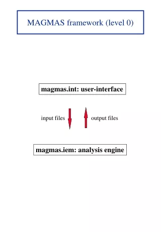
L0DU Functionalities • Aim:Reduce the data flow down to 1 MHz for the next trigger level • The L0DU receives @ 40 MHz information from L0 sub-triggers:- L0 Calorimeter selection board- L0 Muon trigger processor- L0 Pile-Up system • I/O are fully synchronous • A total of 24*32 bits at 40 MHz are expected as input of the L0DU Actually17*32 are used • A physics algorithm is applied to select events and to deliver the L0DU decision @ 40 MHz to the Readout Supervisor
L0DU Outlook • Work on L0DU has started in 1998! • A first prototype (and its test bench) was done in 2002 and successfully tested • 96 inputs; parallel RJ45 …
L0DU Outlook • It was decided to switch to optical inputs (TDR time) • This was not trivial ! • A new prototype (full scale) has been designed in 2004 • Long test phase needed: • We had to learn optical links and their debug • It was necessary to design a dedicated (optical) test bench in July 2005 • Huge over costscovered thanks to special funding from
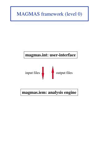
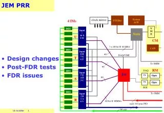
RS Trigger Trigger PC TTCrq RJ45 2 2 2 2 2 USB 304 12 FPGA IInterface&Supervision FPGA Traitement III FPGA Traitement II 32 32 32 L0DU Overview Optical ribbons INPUT data: (24 words 32 bits) Optical links: 16-bit data @ 80 MHz →1.6Gb/s serial data 2x12 fiber ribbons up to 24 inputs HFBR & TLK2501 TTC Single fibers CALO 7 8 2 MUON Patch Panel Pile-Up +7 spares DATA processing: 3 FPGA: • 1: interface & supervisor • 2: treatment
RS Trigger Trigger PC TTCrq RJ45 2 2 2 2 2 USB 304 12 FPGA IInterface&Supervision FPGA Traitement III FPGA Traitement II 32 32 32 L0DU Overview (con’t) OUTPUT data: • RS: 16 bits @ 40 MHz Parallel, 3M connector • HLT: TELL1 Board QTS connectors! L0DU as a TELL1 mezzanine Control data: • From TELL1: CC/PC + JTAG • From external PC:USB L0accept L0accept + Power distribution
RS Trigger Trigger PC TTCrq RJ45 2 2 2 2 2 USB 304 12 FPGA IInterface&Supervision FPGA Traitement III FPGA Traitement II 32 32 32 L0DU Data Flow HLT DATA FLOW From L0DU PGAs To HLT Data sent through TELL1 MAIN DATA FLOW From Trigger processors To Readout Supervisor 100% on the mezzanine CONTROL FLOW From TELL1/CC-PC Or From external PC/USB (independent debugging) L0accept L0accept
L0DU Architecture 7 8 2 7 : 24 words of 32 bits At 40 MHz it receives in parallel: CALO: e,,0L,0G,h,ET,Nspd Muons: 8 cand. Vertex: pile-up 768 bits @ 40MHz 224@40MHz 1024@1MHz OUTPUT: RS, HLT (TELL1)
L0DU Architecture 7 8 2 7 : 24 words of 32 bits • PDP: • Time alignment • Data preparation for algorithms 224@40MHz 1024@1MHz • TDU: • Trigger conditions elaboration • Decision computation OUTPUT: RS, HLT (TELL1)
Flexible Architecture Try to implement a flexible architecture for upgrade, change of algorithms The idea: Set of variables Set of logical operators µ1 µ2 .. e γπ0 h ET Pile-Up > = x + < & … + Threshold can be duplicated several times Possible to combine them “as we’d like” to elaborate a trigger condition (without reprogramming FPGA)
L0DU implementation Patch Panel Patch Panel Ribbon cable GPL L0 DU ODIN Readout Supervisor rack • Slot reserved: • 2 for L0DU • 2 for GPL • 1 spare reserved L0DU Tests • It is mandatory to have a fast an easy L0DU test system and a complete one: • An internal test bench to allow a fast debugging • A dedicated test bench for a full debug based on a Generator Pattern injection for L0DU (GPL) board specially designed for this purpose and permanently available