Download
1 / 2
20 likes | 140 Views
Design and manufacturing of large area, thick cBN films Peter X. Feng, University of Puerto Rico, DMR 0706147.

E N D
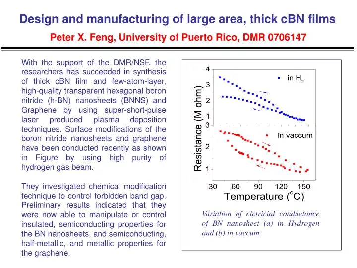
Design and manufacturing of large area, thick cBN films Peter X. Feng, University of Puerto Rico, DMR 0706147 With the support of the DMR/NSF, the researchers has succeeded in synthesis of thick cBN film and few-atom-layer, high-quality transparent hexagonal boron nitride (h-BN) nanosheets (BNNS) and Graphene by using super-short-pulse laser produced plasma deposition techniques. Surface modifications of the boron nitride nanosheets and graphene have been conducted recently as shown in Figure by using high purity of hydrogen gas beam. They investigated chemical modification technique to control forbidden band gap. Preliminary results indicated that they were now able to manipulate or control insulated, semiconducting properties for the BN nanosheets, and semiconducting, half-metallic, and metallic properties for the graphene. Variation of elctricial conductance of BN nanosheet (a) in Hydrogen and (b) in vaccum.
Design and manufacturing of large area, thick cBN films Peter X. Feng, University of Puerto Rico, DMR 0706147 The researchers also spent a significant part of their time for educational activities. It includes visiting local schools, giving talks and demonstrations. For example, they visited and gave talks or demonstrations to four different high schools and one primary school of students in last year. The research team also hosted 5 students from 4 different high schools for two weeks of internship in research laboratory as shown in Figure. The subjects of these modules have far included general physics. A stress is on student involvement and learning through exploration of concepts and ideas. Educational visits and talks to the high school students during internship Through hands-on approach, and attendance of joint group meetings, students have an opportunity to ask questions, and gain insight into how different fields of scientists work together toward a common goal. Students working with those from different but related disciplines would learn the value of cross-disciplinary approaches. All these approaches greatly raise students’ interests in ceramic material research.