Download
1 / 18
180 likes | 188 Views
L6 4211 022142017 ECE 4211 UConn F. Jain LED Design. Design parameters: Operating wavelength, single (green, red, blue) or multi-color white light LEDs Optical power output, expected external and wall conversion efficiency, Cost.: Preferred packaging, (epoxy dome),

E N D
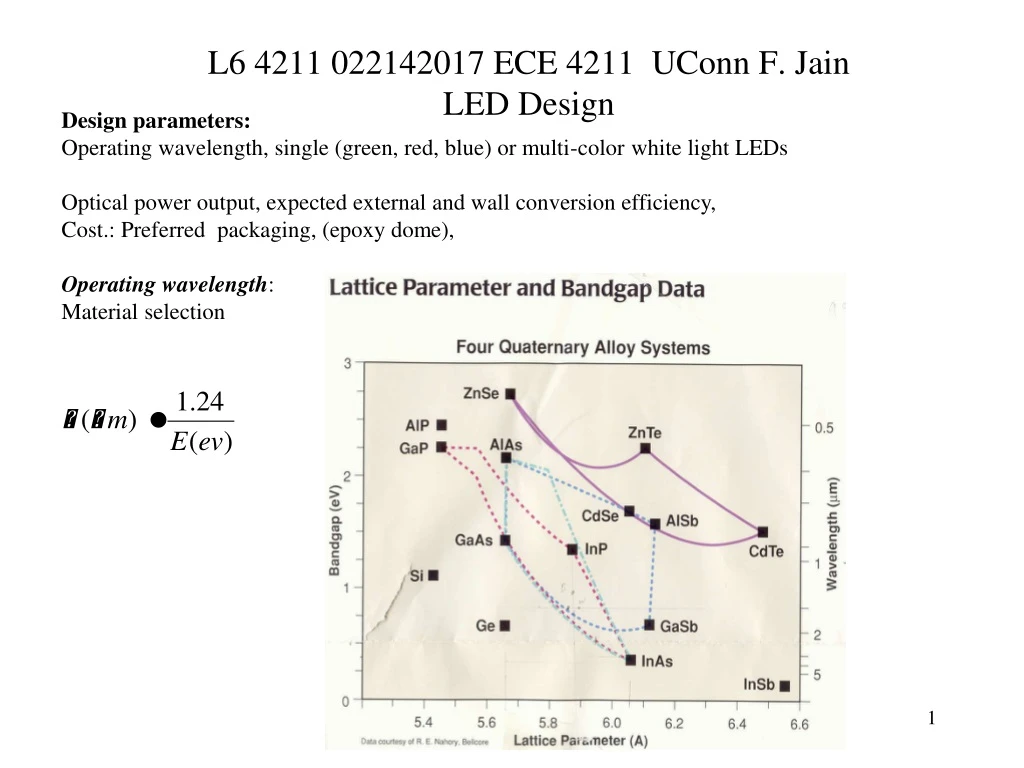
L6 4211 022142017 ECE 4211 UConn F. Jain LED Design Design parameters: Operating wavelength, single (green, red, blue) or multi-color white light LEDs Optical power output, expected external and wall conversion efficiency, Cost.: Preferred packaging, (epoxy dome), Operating wavelength: Material selection
Conventional LED, TIP and InGaN white light LEDs Active layer composition, heterojunction layers, Cladding layers if any, Substrate Cap layers (to lower contact resistance and Ohmic contacts Anti reflection coating and or surface roughening Epoxy dome and/or phosphor layer Overall structure
LED Design Index of refraction for ternary semiconductors 4.7. Refractive Index as a funciton of semiconductor composition This section provides information on the index of refraction for semiconductors we use for visible or infrared sources. The compositional dependence of refractive index in the case of AlxGa1-xAs is given by[1] (22) and for InxGa1-xAsyP1-y[2] [1]H.C. Casey Jr. & M.B. Panish, Heterostructure Lasers Part A: Fundamental Principles, Academic Press, 1978, Chapter 2 [2]G.H.Olsen et al, Journal of Electronic Materials, vol 9, pp. 977-987, 1980.
P-GaP Cap layer (Window) Eg3 =2.24 P-AlGaInP (Eg2) 2.1ev P-AlGaInP (Eg1 different composition) n AlGaInP (Eg2) Eg3 > Eg2 > Eg1 Lift-off layer/buffer (Sacrificial) n-GaAs Substrate 1.42ev Fig 6. Epi layer transfer from GaAs to GaP substrate Double Heterostructure (DH) LED Epoxy Dome Ohmic contact toSubstrate n-GaP Substrate Material selection DH LED AlGaInP W=1.5 2Ln=7.1*2=14 p-GaP Cap Contact Ohmic Fig 7. Truncated inverted pyramid (TIP) LED with 50% Extraction efficiency hextraction Double Heterojunction
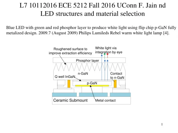
Fig. 7 Blue LED with green and red phosphor layer to produce white light using flip chip p-GaN fully metalized design. 2009.7 (August 2009) Philips Lumileds Rebel warm white light lamp [4].
Performance parameters:[4] Operating conditions— Current I = 700 mA, area 1mm2, V=3.2V DC. Cumulative white light efficiency hL = 14%. It is composed of three terms. 1. Blue LED efficiency-- hB = 0.73W/2.24W = 33%. 2. Phosphor package efficiency hP = 0.4 W/0.73W = 54%. 3. Spectral efficacy hS = 128 lm/164 lm =78%. (it measures response of eye). Power Budget: DC power 2.2W (VI=0.7A *3.2V) is supplied by the power supply. 1. It produces 0.73W of light having following components • 0.511 W blue photons input used by red phosphor which produces 0.263 W and out put is at 29% after various losses. • 0.177 W blue power input is used by green phosphor which produces 0.104 W and after accounting for various losses, we are left with 18%, • 0.046 W remaining blue input produces 0.036W). The losses in phosphor are due to Stokes loss (input at high energy and out put at low), scattering and absorption losses. 2. 0.39W is lost due to voltage droop due to reduction of internal quantum efficiency as compared with obtained under low injection condition (1- hIQE/ hIQE, lo inj), 30%. 3. Internal non-radiative transitions 0.56W (30%); (1- hIQE, lo inj). 4. Joule loss 0.3W (15%) 5. Un-extracted light (1- hEQE), here hEQE is external quantum efficiency. Operating voltage V and current I to design a LED DC power P (V*I) = Optical power emitted/ Po supplied by battery= DC power P (V*I) + I2R losses
DC power P (V*I) = Optical power emitted/ External efficiency Po supplied by battery= DC power P (V*I) + I2R losses
Internal efficiency (1) 50% Loss due to travel towards the back contact Figure 14 shows that about 1/2 of the generated light is lost as it travels towards the back electrode. 2. Surface reflection 3. Critical angle related loss Improve Extraction efficiency
Overall conversion efficiency Overall Conversion Efficiency Overall efficiency is defined as the Light output (integrated in all directions) in watts/Electrical power input (VI) supplied to the device. Sometimes the power conversion efficiency is defined as Here, P(λ) = light output at wavelength
Tuning of band gap by strain Ref: W. Huang, 1995 UConn doctoral thesis with F. Jain • Under the tensile strain, the light hole band is lifted above the heavy hole, resulting in a smaller band gap. • Under a compressive strain the light hole is pushed away from heavy. As a result the effective band gap as well as light and heavy hole m asses are a function of lattice strain. Generally, the strain is +/- 0.5-1.5%. "+" for tensile and "-" for compressive. • Strain does not change the nature of the band gap. That is, direct band gap materials remain direct gap and the indirect gap remain indirect.
Material Selection Point A: Project GaAs-A-InAs curve on the horizontal O-C-2 line. Find the fraction OC/O2 = 0.528 C2/O2 = 0.472. Therefore, at point A the composition is Ga0.472In0.528As.
4.8. Methods to Reduce Losses in LEDs Various mechanisms are identified which lead to losses of generated photons in a p-n diode. Design methods are outlined to reduce these losses. We have seen that if all the loss mechanisms are considered, the light extraction efficiency comes out to be very low (1-2%). The following steps are taken to reduce photon losses ( or improve photon extraction): • To recover part of the photons traveling towards the bottom contact. There are various ways to achieve this. One may be have a reflecting contact. This invariably results in poor electrical characteristics; due to increased Ohmic voltage drop (contact resistance * current). Another way is to incorporate a layer, shown dotted in Figure 16, having a lower index of refraction than the layer in which the photons are generated.
LED Design Index of refraction for ternary semiconductors 4.7. Refractive Index as a funciton of semiconductor composition This section provides information on the index of refraction for semiconductors we use for visible or infrared sources. The compositional dependence of refractive index in the case of AlxGa1-xAs is given by[1] (22) and for InxGa1-xAsyP1-y[2] [1]H.C. Casey Jr. & M.B. Panish, Heterostructure Lasers Part A: Fundamental Principles, Academic Press, 1978, Chapter 2 [2]G.H.Olsen et al, Journal of Electronic Materials, vol 9, pp. 977-987, 1980.