Download
1 / 18
180 likes | 186 Views
This study presents a solution to reduce leakage current in III-V MOSFETs for low power logic, using InP recessed source/drain spacers. The implementation of wide-band-gap barriers, vertical spacers, ultrathin channels, and doping-graded InP spacers effectively improves device performance. The research was supported by SRC Non-classical CMOS Research Center and NSF-funded NNIN network.

E N D
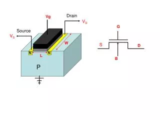
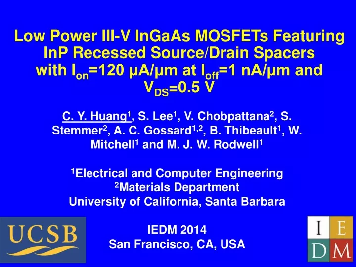
Low Power III-V InGaAs MOSFETs Featuring InP Recessed Source/Drain Spacers with Ion=120 μA/μm at Ioff=1 nA/μm and VDS=0.5 V C. Y. Huang1, S. Lee1, V. Chobpattana2, S. Stemmer2, A. C. Gossard1,2, B. Thibeault1, W. Mitchell1 and M. J. W. Rodwell1 1Electrical and Computer Engineering 2Materials Department University of California, Santa Barbara IEDM 2014 San Francisco, CA, USA
Outline • Problem: III-V MOSFETs are very leaky • Gate-last Process Flow • Knob 1: Wide band-gap barrier • Knob 2: Source/Drain vertical spacer • Knob 3: Ultrathin channel • Knob 4: Recessed InP S/D spacer • Knob 5: Doping-graded InP spacer • Summary 2
InGaAs/InAs FETs are leaky! • III-V channel: low electron effective mass, high velocity, high mobility higher current at lower VDD • Low band gap band-to band tunneling (BTBT) • High permittivity worse electrostatics, large DIBL • Goal: reduce leakage current for low power logic! S. Lee et al., VLSI 2013 3
Wide band-gap barriers or P-doped back barriers reduces bottom leakage path. • Solution 1: AlAsSb barriers (Sample B) reduces subthreshold leakage. • Solution 2: P-doped InAlAs barriers also work well. Knob 1: Wide Band-gap Barrier C. Y. Huang et al., APL., 103, 203502 (2013) 5
Knob 2: Source/Drain Vertical Spacer S. Lee et al., APL 103, 233503 (2013) C. Y. Huang et al., DRC 2014. Vertical spacers reduce the peak electric field, improve electrostatics, and reduce BTBT floor. 6
Knob 3: Ultra-thin channel S. Lee et al., VLSI 2014 7
Increasing band gap: In0.53Ga0.47As channel BTBT limited Reducing channel thickness improves electrostatics, increases confinement bandgap and reduces BTBT. 8
E-field and BTBT contour R. Chu et al., EDL 29, 974 (2008) J. Lin et al., EDL 35, 1203 (2014) • Concentrated electric field at the drain end of the channel next to the gate edge. • Solution: • Replace InGaAs with wide band-gap InP (Eg~1.35 eV) 9
Knob 4: Recessed InP S/D spacer 12 nm InGaAs spacer 5 nm Recessed InP spacer Lg-60 nm 10
InP spacer thickness: subthreshold • Minimum spacer thickness is required to maintain good electrostatics. • Thicker spacer is desired at drain to smooth electric field. 11
InP spacer thickness: on-state • Thicker InP spacer increases Ron, and degrades Gm • Thinner spacer is desired at source to reduce RS/D. 12
Knob 5: Doping-graded InP spacer Lg-30 nm, 30Å ZrO2 • Doping-graded InP spacer reduces parasitic source/drain resistance and improves Gm. • Gate leakage limits Ioff~300 pA/μm. 13
Doping-graded InP spacer+Thicker oxide InP graded spacer InGaAs spacer 38Å ZrO2 60 pA/μm • Minimum Ioff~ 60 pA/μm at VD=0.5V for Lg-30 nm • 100:1 smaller Ioff compared to InGaAs spacer 14
Ion vs Lg at Ioff = 1 nA/μm Ion/Ioff~1.5x105 • Peak Ion= 150 µA/µm at VDS=0.5V for Lg-45 nm devices. 15
Ion vs Lg at Ioff = 100 nA/μm • Peak Ion= 415 µA/µm at VDS = 0.5V for this work. • Ultrathin InAs channel shows highest Ion. 16
Ion= 150 µA/µm at Ioff = 1 nA/µm Ion= 500 µA/µm at Ioff = 100 nA/µm 17
Recessed InP source/drain spacers enable III-V MOSFETs for low power logic. Thank you! • This research was supported by the SRC Non-classical CMOS Research Center (Task 1437.009) and GLOBALFOUNDRIES(Task 2540.001). • A portion of this work was done in the UCSB nanofabrication facility, part of NSF funded NNIN network. • This work was partially supported by the MRSEC Program of the National Science Foundation under Award No. DMR 1121053. 18