Download
1 / 19
190 likes | 347 Views
超平坦 GaAs 量子井戸の発光像とスペクトル計測. Ji-Won Oh , Masahiro Yoshita , Hirotake Itoh , Hidefumi Akiyama, Loren Pfeiffer A , Ken West A Institute for solid state physics, University of Tokyo,and CREST, JST Bell Laboratories, Lucent Technologies, USA. A. Introduction.

E N D
超平坦GaAs量子井戸の発光像とスペクトル計測超平坦GaAs量子井戸の発光像とスペクトル計測 Ji-Won Oh,Masahiro Yoshita,Hirotake Itoh,Hidefumi Akiyama, Loren PfeifferA,Ken WestA Institute for solid state physics, University of Tokyo,and CREST, JST Bell Laboratories, Lucent Technologies, USA.A
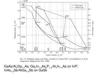
Introduction • Novelgrowth-interrupt annealing technique with a cleaved-edge overgrowth (CEO) method in MBE growth:Atomically flat (110) GaAs quantum well • [1] M. Yoshita, H. Akiyama, L. N. Pfeiffer, K. W. WestJpn. J. Appl. Phys. 40, L252-254 (2001). • Slight variation in Ga supply results in the formation of characteristic surface step-edge patterns such as 2- or 3-ML high- islands or 1-ML-deep pits • [2] M. Yoshita, H. Akiyama, L. N. Pfeiffer, K. W. West, Appl. Phys. Lett. 81, 49-51 (2002) 600 ℃ 10 min 5X5mm
Characteristic Surface Forms on Atomically Flat Surface 2- or 3-ML high islands [110] 1-ML-deep pits [001] [3] J. W. Oh, M. Yoshita, H. Akiyama, L. N. Pfeiffer, K. W. West,Appl. Phys. Lett. 82, 1709-1711,2003. Applied Physics Letters表紙論文!
Purpose of experiment Carrier diffusionon atomically flat (110) GaAs /GaAlAs QW and its dependences on temperature (4K-120K) observed by point and uniform optical excitation by Ti-Sa laser (730nm)
Schematic Diagram for PL observation at various sample position & temperatures Ti-Sa PL Temp 4K 10K 30K 45K 60K 90K 100K 120K 10nm Atomically Flat (110) ! 10nm 6nm 6.8mm GaAs 29% AlGaAs AlGaAs
Image of 1-ML Deep Pits 4K 10K 30K 45K 60K 80K 100K 120K mm
Image and PL spectra of 2-3 ML High Islands 4K 10K 30K 45K 60K 80K 100K 120K mm
Atomically Flat (110) Surface 4K 10K 30K 45K 60K 80K 100K 120K mm
Sliced PL Profiles from Atomically Flat Surface gets thinner
Measurement of Diffusion Length at various lowtemperature with point excitation PL Reflection image 1mm FWHM:0.95mm 6.8mm
Spot PL images at various low temperature 30K 4K 2mm 60K 100K :Beam Reflection PL Image
Diffusion on Atomically Flat surface At 30K t=4000 ps m=4000 By Hilmer et. al. Phys. Rev. B.42. 3220-3223 (1990) in our data Longer diffusion length
Conclusion ・Observation of unique surface forms on atomically flat (110) interface in GaAs/GaAlAs QW via microscopic PL imaging 1-ML-deep pits: dark triangular regions (higher energy regions: carriers flow outside) 2~3 ML-high islands :bright PL spots (lower energy regions: carriers flow inside) ・ Carrier diffusion length in low temp. by point excitation : efficient carrier migration over 1 mm scale even at 4K which increases with temp ・ Slenderizing PL image with growing temp: well explained by the measured
Characterizing top surface of Sample with AFM 80mm 29.X ML As 3~4 mm 30.0 ML [110] 30.X ML Ga [001] [110]
Fabrication of QW sample by cleaved-edge overgrowth GaAs QW (110) First MBE growth Second MBE growth in situ cleavage 1 GaAs (001) substrate (001)
Abstract By means of cleaved-edge overgrowth method with molecular beam epitaxy and growth interrupt annealing, we fabricated (110) GaAs quantum wells having atomically flat interfaces. We introduced characteristic 1-ML-deep pits and 2~3-ML-high islands on atomically flat interfaces by adding fractional monolayer of GaAs, which are characterized by atomic force microscope (AFM). In PL observation with uniform excitation, pits are reproduced as dark triangle images due to higher energy than surroundi- ngs and islands as bright PL spots due to lower energy. With increasing temperature, we observe changes in their shape and enhanced contrast, which is explained by enhanced carrier diffusion length due to significant reduction of interface-roughness scattering.
04-d 06-c 01-b 10-c 11-c 09-c Ga-24