Download
1 / 20
200 likes | 204 Views
This lecture covers the concept of programmable logic devices (PLDs), including PLAs, PALs, and ROMs. It explains the structure and programming of PLDs and compares PLAs and PALs. The lecture also discusses the use of ROMs and their advantages and limitations.

E N D
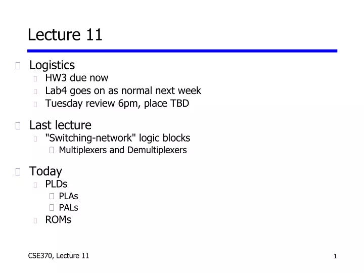
Lecture 11 • Logistics • HW3 due now • Lab4 goes on as normal next week • Tuesday review 6pm, place TBD • Last lecture • "Switching-network" logic blocks • Multiplexers and Demultiplexers • Today • PLDs • PLAs • PALs • ROMs
The “WHY” slide • Programmable Logic Devices (PLDs) • Often you want to have a look up table of functions stored away somewhere in your device. Rather than having specific circuits build every time, it would be nice to have a “general-purpose” structure that could be “programmed” for a specific usage. PLDs have a generic structure that allows any function to be expressed and stored. • And it is nice if it is reprogrammable. Some PLDs are reprogrammable (like your memory sticks).
Programmable logic (PLAs & PALs ) • Concept: Large array of uncommitted AND/OR gates • Actually NAND/NOR gates • You program the array by making or breaking connections • Programmable block for sum-of-products logic • • • inputs ANDarray ORarray productterms outputs • • •
Programming the wire connections • Fuse: Comes connected; break unwanted connections • Anti-fuse: Comes disconnected; make wanted connections B C A F0 = A + B'C' F1 = AC' + AB F2 = B'C' + AB F3 = B'C + A AB B'C AC' B'C' A 1 F0 F1 F2 F3
Short-hand notation • Draw multiple wires as a single wire or bus • × signifies a connection Before Programming After Programming A B C D AB A'B' CD' C'D F0 = AB + A'B' F1 = CD' + C'D F0 F1
A B C A'B'C' A'B'C A'BC' A'BC AB'C' AB'C ABC' ABC F1 F2 F3 F4 F5 F6 PLA example F1 = ABC F2 = A + B + C F3 = A' B' C' F4 = A' + B' + C' F5 = A xor B xor C F6 = A xnor B xnor C Think of as a memory-address decoder Memory bits A B C F1 F2 F3 F4 F5 F6 0 0 0 0 0 1 1 0 0 0 0 1 0 1 0 1 1 1 0 1 0 0 1 0 1 1 1 0 1 1 0 1 0 1 0 0 1 0 0 0 1 0 1 1 1 1 0 1 0 1 0 1 0 0 1 1 0 0 1 0 1 0 0 1 1 1 1 1 0 0 1 1
PLAs versus PALs • We've been looking at PLAs • Fully programmable AND / OR arrays • Programmable array logic (PAL) • Programmable AND array • OR array is prewired • Cheaper and faster than PLAs
Example: BCD to Gray code converter A B C D W X Y Z0 0 0 0 0 0 0 00 0 0 1 0 0 0 10 0 1 0 0 0 1 10 0 1 1 0 0 1 00 1 0 0 0 1 1 00 1 0 1 1 1 1 00 1 1 0 1 0 1 00 1 1 1 1 0 1 11 0 0 0 1 0 0 11 0 0 1 1 0 0 01 0 1 0 X X X X1 0 1 1 X X X X 1 1 0 0 X X X X 1 1 0 1 X X X X 1 1 1 0 X X X X 1 1 1 1 X X X X A A AB AB 00 01 11 10 00 01 11 10 CD CD 00 0 0 X 101 0 1 X 111 0 1 X X10 0 1 X X 00 0 1 X 001 0 1 X 011 0 0 X X10 0 0 X X D D C C B B K-map for W K-map for X A A AB AB 00 01 11 10 00 01 11 10 CD CD 00 0 1 X 001 0 1 X 011 1 1 X X10 1 1 X X 00 0 0 X 101 1 0 X 011 0 1 X X10 1 0 X X D D C C B B K-map for Y K-map for Z
A B C D W X Y Z Example: BCD to Gray --- Wire a PLA Minimized functions: W = A + BC + BD X = BC' Y = B + C Z = A'B'C'D + BCD + AD' + B'CD'
Example: Wire a PAL Minimized functions: W = A + BC + BD X = BC' Y = B + C Z = A'B'C'D + BCD + AD' + B'CD’ Fine example for the use of PAL (because no shared AND terms) Many AND gates wasted, but still faster and cheaper than PLA
Compare implementations for this example • PLA: • No shared logic terms in this example • 10 decoded functions (10 AND gates) • PAL: • Z requires 4 product terms • 16 decoded functions (16 AND gates) • 6 unused AND gates • This decoder is a best candidate for PLAs/PALs • 10 of 16 possible inputs are decoded • No sharing among AND terms • Another option? • Yes — a ROM
Read-only memories (ROMs) • Two dimensional array of stored 1s and 0s • Input is an address ROM decodes all possible input addresses • Stored row entry is called a "word" • ROM output is the decoded word n address lines • • • inputs memoryarray(2n wordsby m bits) 2n wordlines decoder outputs • • •
ROM details • Similar to a PLA but with a fully decoded AND array • Completely flexible OR array (unlike a PAL) • Extremely dense: One transistor per stored bit +5V Only one word line is active at any time n-1 2 2 decoder 1 0 0 n-1 Address 0 m-1 Outputs Bit lines: Normally pulled high through resistor. If transistor stores a zero, then line pulls low when row is selected
Two-level combinational logic using a ROM • Use a ROM to directly store a truth table • No need to minimize logic • Example: F0 = A'B'C + AB'C' + AB'C • F1 = A'B'C + A'BC' + ABC • F2 = A'B'C' + A'B'C + AB'C' • F3 = A'BC + AB'C' + ABC' A B C F0 F1 F2 F3 0 0 0 0 0 1 00 0 1 1 1 1 00 1 0 0 1 0 00 1 1 0 0 0 1 1 0 0 1 0 1 1 1 0 1 1 0 0 0 1 1 0 0 0 0 1 1 1 1 0 1 0 0 You specify whether to store 1 or 0 in each location in the ROM ROM8 words x 4 bits/word A B C F0 F1 F2 F3 address outputs
ROMs versus PLAs/PALs • ROMs • Benefits • Quick to design, simple, dense • Limitations • Size doubles for each additional input • Can't exploit don't cares • PLAs/PALs • Benefits • Logic minimization reduces size • PALs faster/cheaper than PLAs • Limitations • PAL OR-plane has hard-wired fan-in • Another alternative: Field programmable gate arrays • Learn a bit more later in this class
c0 c1 c5 c6 c4 c2 c3 Example: BCD to 7-segment display controller • The problem • Input is a 4-bit BCD digit (A, B, C, D) • Need signals to drive a display (7 outputs C0 – C6) c0 c1 c2 c3 c4 c5 c6 BCD to 7–segmentcontrol-signaldecoder A B C D
Formalize the problem • Truth table • Many don’t cares • Choose implementation target • If ROM, we are done • Don't cares imply PAL/PLA may be good choice • Implement design • Minimize the logic • Map into PAL/PLA A B C D C0 C1 C2 C3 C4 C5 C6 0 0 0 0 1 1 1 1 1 1 0 0 0 0 1 0 1 1 0 0 0 0 0 0 1 0 1 1 0 1 1 0 1 0 0 1 1 1 1 1 1 0 0 1 0 1 0 0 0 1 1 0 0 1 1 0 1 0 1 1 0 1 1 0 1 1 0 1 1 0 1 0 1 1 1 1 1 0 1 1 1 1 1 1 0 0 0 0 1 0 0 0 1 1 1 1 1 1 1 1 0 0 1 1 1 1 0 0 1 1 1 0 1 X X X X X X X X 1 1 X X X X X X X X X
A A A A A A A 1 1 X 1 1 1 X 1 1 1 X X 0 1 X X 1 1 X 1 0 1 X 1 0 0 X X 0 1 X X 1 0 X 1 0 1 X 0 1 0 X X 1 1 X X 1 0 X 1 0 0 X 0 0 0 X X 1 1 X X 1 0 X 1 0 1 X 1 1 1 X X 1 1 X X 1 1 X 1 1 0 X 1 1 1 X X 1 0 X X 0 1 X 1 0 1 X 1 1 0 X X 1 1 X X D D D D D D D C C C C C C C B B B B B B B Sum-of-products implementation • 15 unique product terms if we minimize individually C0 = A + B D + C + B' D' C1 = C' D' + C D + B' C2 = B + C' + D C3 = B' D' + C D' + B C' D + B' C C4 = B' D' + C D' C5 = A + C' D' + B D' + B C' C6 = A + C D' + B C' + B' C 4 input, 7 output PLA: 15 AND gates PAL: 4 product terms per output (28 AND gates)
A A 1 1 X 1 1 1 X 1 1 1 X X 0 1 X X 1 1 X 1 1 1 X 1 1 1 X X 0 1 X X D D C C B B If choosing PLA: better SOP implementation • Can do better than 15 product terms • Share terms among outputs only 9 unique product terms • Each term not necessarily minimized C2 C2 C0 = A + BD + C + B'D' C1 = C'D' + CD + B' C2 = B + C' + D C3 = B'D' + CD' + BC'D + B'C C4 = B'D' + CD' C5 = A + C'D' + BD' + BC' C6 = A + CD' + BC' + B'C C0 = BC'D + CD + B'D' + BCD' + AC1 = B'D + C'D' + CD + B'D'C2 = B'D + BC'D + C'D' + CD + BCD'C3 = BC'D + B'D + B'D' + BCD'C4 = B'D' + BCD'C5 = BC'D + C'D' + A + BCD'C6 = B'C + BC' + BCD' + A
PLA implementation C0 = BC'D + CD + B'D' + BCD' + AC1 = B'D + C'D' + CD + B'D'C2 = B'D + BC'D + C'D' + CD + BCD'C3 = BC'D + B'D + B'D' + BCD'C4 = B'D' + BCD'C5 = BC'D + C'D' + A + BCD'C6 = B'C + BC' + BCD' + A A B C D BC' B'C B'D BC'D C'D' CD B'D' A BCD' C0 C1 C2 C3 C4 C5 C6 C7