Download
1 / 16
160 likes | 163 Views
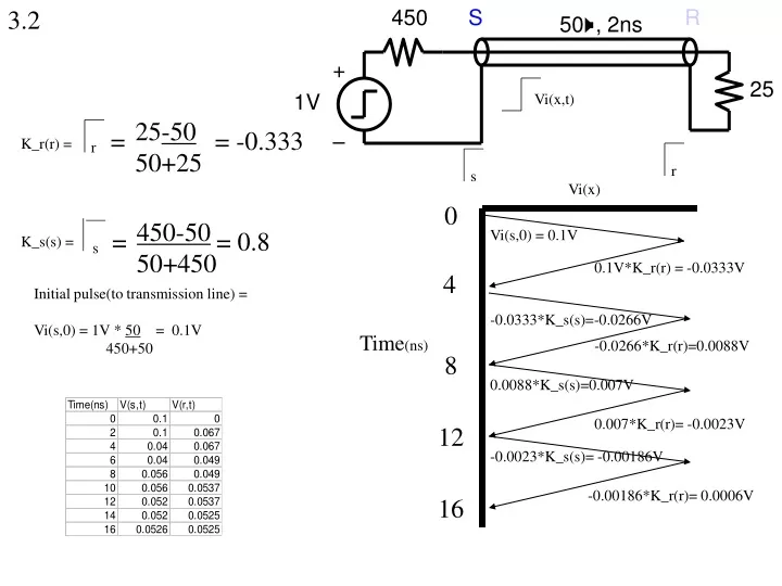
3.2. 450. S. R. +. –. 50 W , 2ns. 25. 1V. Vi(x,t). 25 -50 50+25. =. = -0.333. K_r(r) =. r. r. s. Vi(x). 0. 450-50 50+450. =. = 0.8. Vi(s,0) = 0.1V. K_s(s) =. s. 0.1V*K_r(r) = -0.0333V. 4. Initial pulse(to transmission line) = Vi(s,0) = 1V * 50 = 0.1V

E N D
3.2 450 S R + – 50W, 2ns 25 1V Vi(x,t) 25-50 50+25 = = -0.333 K_r(r) = r r s Vi(x) 0 450-50 50+450 = = 0.8 Vi(s,0) = 0.1V K_s(s) = s 0.1V*K_r(r) = -0.0333V 4 Initial pulse(to transmission line) = Vi(s,0) = 1V * 50 = 0.1V 450+50 -0.0333*K_s(s)=-0.0266V Time(ns) -0.0266*K_r(r)=0.0088V 8 0.0088*K_s(s)=0.007V 0.007*K_r(r)= -0.0023V 12 -0.0023*K_s(s)= -0.00186V -0.00186*K_r(r)= 0.0006V 16
3.2 Vs Vr
3.8 In this question, we basically use the idea of the probe stub toallow us to design a multidrop bus. A bus must communicate fromthe bus to the driver, and also from the driver to the bus. In order todo this, we need to terminate the stub at the driver itself, which is why the book refers to using a source-terminated driver. 50W 50W 50W BUS Ratten Ratten driver driver 50W 50W 50W 50W There are two different directions of signals and their corresponding attenuations. One: how much voltage appearson the bus created from a signal driven by driver to the bus? Two: how much voltage appears at the driver givena voltage on the bus. How much of this signal is attenuated by the stubs?
50W R1 50W BUS V2(t) V1(t) V1(t)=1V K_r V4(t) Ratten V2(t)=.976V transceiver V3(t) 50W 50W K_r*V1(t)=-0.024V Let’s first look at direction of a signal traveling from the bus to the driver/receiver. Let’s first assume that Ratten= OO(infinity).In this situation, R1=50Ohms||OO=50 Ohms. So, we see no reflection and the inital pulse V1(t) just propagates down the bus, without any power dissipation in the probe stub. However, if Ratten=950 Ohms, then R1=(950+50)||50= 47.6Ohms Because R1= 50 Ohms, we know that there will be a reflection here. ==>K_R=-0.024. So a reflected wave of -0.024*V1==> V2(t)(voltage that propagates down the line)=(1-0.024)*V1(t)=0.976*V2(t). So, decreasing Ratten increases the amount of attenuation that we see for a signal traveling along the bus. What happens to the signal that now travels through the probe stub? Well, V3(t)~ V1(t) * 50 50 + RattenSo, for Ratten = 950 Ohms, V3(t)=1/20. Hence, the 20:1 attenuation. Here, we see that depending on the value of Ratten, our attenuation from the one end of the bus to the other end of the bus is inversely proportional to the attenuation from the bus to the driver/receiver stub. ==> Attenuation to the transceiver = Ratten + 50 Attenuation of bus = V1(t) where K_R=R1-50 50 (1+tauR)V1(t) R1+50 where R1=(Ratten+50)||50
We also need to determine home much voltage we see on the bus when we apply a voltage V4(t) from the transceiver. Thisis akin to a driver driving a value onto the bus. Basically, what is the value of V6(t) for applying V4(t). Well, V5(t) = V4(t)/2 ==> Rin=Ratten+25 ==> K_R = Rin - 50 Rin + 50 Vi = (1+K_R)*V5(t) ==> V6(t) = 50||50 * Vi 50||50 + Ratten==> V6(t) = 50||50 * (1+K_R)*V4(t)/2 50||50 + Ratten So, by increasing the value of Ratten, we also are degrading our signal that is traveling from the driver to the bus. 50W V6(t) 50W Ratten V4(t) Vi Rin Driver/Receiver K_R 50W 50W V5(t)
10-50 50+10 + 1V – = = -0.66 50W, 2ns K_r(r) = 10W s r r Initial pulse(to transmission line) = Vi(s,0) = 1V * 50 = 0.833V 10+50 1V Vi(x,t) At the beginning of time, V(r)=0V. Assume that both diodesare not conducting. In this case, V(r) looks like an open circuit.A wave of 0.83V hits the end of the line. Nominally, for an opencircuit, the wave will get reflected back with K_r(r)=1. That meansthat V(r)=1.66V. However, we know that once V(r)=1V, the topdiode becomes conducting, forcing V(r)=1V. Therefore, it is impossible for 0.83V to reflect back. Instead, a wave of 1-0.83V=0.17V is reflected backwards to V(s), in order for V(r)=0.83V+0.17V=1V. This 0.17V is now a traveling wave back to the source, where it sees a negative reflection coefficient, so that a -0.66*0.17=-0.112V wave now is heading towards V(r). However, when this wave hits V(r), since the top diode is conducting, K_r(r)=-1. So this -0.112V gets reflected back as a wave of magnitude 0.112V. This basically “rings” up the source voltage, while V(r)rings up with the inital step voltage. s Vi(x) r 0 Vi(s,0) = 0.833V 0.17V 4 0.17*K_s(s)=-0.112V -0.112*K_r(r)=0.112V 8 0.112*K_s(s)=-0.074V -0.074*K_r(r)= 0.074V 12 0.074*K_s(s)= -0.049V -0.049*K_r(r)= 0.049V 16 Time(ns)
You can also consider the reflection process with currents as opposed to voltages ringing along the line.The initial pulse puts a current of 1V/60 = 16.6mA into the line. At the far end, which is terminated bythe diodes, 3.4mAreflects back and 13.2mA goes into the diode. When the 3.4mA reaches the source, -2.2mA reflects back. When this gets to the far end, it reduces the 13.2mA to 11.0mA, but since this is greater than 0 the diode remains conducting and a negative reflection occurs -- reducing the diode current to 8.8mA. And so on. The following spice waveform shows what happens when the diode connected system is input with a much slower input step edge.(200ps vs 10ps) Since the input voltage doesn’t rise to 1V fast enough, the input into the line will not be an immediate 0.83V, but instead, a slower rise to 0.83V. This means that the reflection at the end of the line will see an open circuit for longer time, since the pulse doesn’t rise to 0.83V that fast. In this manner, you see the reflected pulses from the transmitter termination go to 1V and then settle back to the values that were calculated above, due to the finite time of the input rise time.
+ – 50 50, 66ps 60, 133ps 60, 133ps 5nH 50 Vi(x,t) 1pF 2V 3pF Let’s first calculate the transmission line segments. We know the first segment consists of a source resistance of 50 Ohms, in series with a tranmission line of 50 Ohms. This is because we know that the step voltage is 2V and V(s)=1V, meaning there is a pure resistive divider=>2V*50/100 = 1V. We know this first tranmission line is 66ps long, because thepoint where we begin to see the capacitance is about 132ps away from the inital inputvoltage step. Therefore, Td=132/2=66ps. The second transmission line segment is 133ps long. We can estimate this amount by observing the distance in time the inductance is from the source voltage. From the graph, it seems that the upward inductance step is 400ps away from the source, meaning that 2*66ps+2*133ps=400ps. Finally, the downward dip of the last capacitance is about 660ps away from the 10ns inputvoltage step=> 2*66ps+2*133ps+2*133ps= 664ps. So, the lengths of the transmissionlines are correct.
We know that the first transmission line is 50 Ohms, since there’s no reflection at the input voltage step. We can solve for the second tranmission line, since the voltage along the second tranmission line is 1.1V. ==> Z2 - 50 = 0.1 Z2=61 Ohms. Z2 + 50 The third transmission line segment also settles to around 1.1V, so this segment is also 61 Ohms, although this is a little more difficult to determine. Capacitor 1 To calculate the first capacitance, we can use either the equations in the book(3-69, simplifiedto 3-79), or use the area integration method seen from lecture. We’ll do both here. Tau(time constant of C1) = tr*deltaV / [1-exp(-tr/tau)] [eq 3-69] V Use the above to iterate for Tau above.==>deltaV=0.8V, tr=10ps. (assuming you know what “iterating” for solution means.) From above, get tau=21ps. ==>tau = Reff*C1 ==>Reff~50||50 = 25Ohms. Therefore, C1 ~ 840ff. Which is close to the above of 1pF.
Inductor 1To find the first inductor, again we estimate the value of the peaking by the formula above.One simplification we have now, however, is that our rise time has been degraded(from thefast input step of 0.01ns). The input step is probably around 50-100ps now, which is the “rise” time of the RC capacitor charging. This is the waveform that is actually passingthrough the inductor. The initial step input into the inductor probably looks like the risingportion of the RC. In this situation, tr is probably much greater than tau, so we can use thesimplified formula of 3-79. ==> tr=100ps, deltaV=0.35V. (note:V in the denominator~0.8-0.9V) ==> tau=tr*deltaV/V = 44ps. Knowing that the impedance seen by the inductor is 2Z0, the time constant for the inductor is TauL*2*Z0=L= 44ps*2*60=5.3nH, which is close to 5nH. Capacitor 2 For the final capacitor, it’s going to get harder to figure it out, due to the degradation in rise time. Let’s guess that the final capacitor has an input step of tr=250ps.(try to guess this by the L/R time constant of the inductor) Again, by using Tau=tr*deltaV/V ==>Tau~250ps*0.3V/0.5V=150ps. Again, assuming that the capacitor sees two tranmission lines in parallel(Z0~50), from 3-67, C=tau*2/Z0=5pF. This is “somewhat” close to what is there. It becomes quitehard to figure out what the value is. The best approach is to basically start iterating in SPICE the final value of the capacitor.
Capacitor 1 You can also solve for the capacitor 1 by estimating the area under the curve. Using a similar analysis to the handout given in the problem session, we found that Lw=4*Z0*Area Similarly, deriving through the integration equation, or knowing the V0 duality between inductance and capacitance, we know: Cw=2*A where V0=1V, Zeff=50||50 = 25 Ohms Zeff*V0 The area under the curve is approximately 0.5*(10.17ns-10.13ns)*0.8V plugging in, ==> Cw=1.28pF, which is close to the 1pF shown above.