Download
1 / 20
250 likes | 271 Views
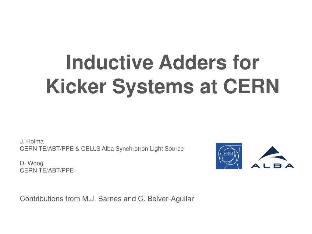
Inductive Adders for Kicker Systems at CERN. J. Holma CERN TE/ABT/PPE & CELLS Alba Synchrotron Light Source D. Woog CERN TE/ABT/PPE. Contributions from M.J. Barnes and C. Belver-Aguilar. Outline. Inductive Adder Topology Schematic and features CLIC DR Kicker Inductive Adders

E N D
Inductive Adders for Kicker Systems at CERN J. Holma CERN TE/ABT/PPE & CELLS Alba Synchrotron Light Source D. Woog CERN TE/ABT/PPE Contributions from M.J. Barnes and C. Belver-Aguilar
Outline • Inductive Adder Topology • Schematic and features • CLIC DR Kicker Inductive Adders • Specifications • Active Analogue Modulation • Measurements on Prototype Inductive Adders: • Future Work PULPOKS 2018 J. Holma
Magnetic core Inductive Adder Pulse capacitor PCB • Many primary “layers”, each with solid-state switches • The output voltage is (approximately) the sum of the voltages of the primary constant voltage layers • + Possibility to generate positive or negative output pulses with the same adder: the polarity of the ouput pulses can be easily changed by grounding the other end of the output of the adder • + All control electronics referenced to ground potential. • + The output voltage can be modulated during the pulse by passive/active analogue modulation. • + Built-in fault tolerance and redundancy: if one switch or layer fails, the adder still gives full voltage or a significant portion of the required output pulse (good for the machine safety). • +Modularity: the same design can potentially be used for CLIC DR & PDR kicker modulators and combined extraction + dump kicker (12.5/17.5 kV) • - Pulse duration limited by Volt x second product of the magnetic cores • - Residual voltage after the pulse (demagnetization of the magnetic cores) MOSFET switch Secondary PULPOKS 2018 J. Holma
CLIC DR Extraction Kicker System • Stripline kicker: both electric and magnetic fields deflect the beam. • Two inductive adders needed to generate positive and negative pulses for stripline electrodes • Impedance of each electrode is 50 𝛺 when “off” (even mode) and 40.5 𝛺 when “on” (odd mode): both modes are matched with a terminating resistor network. • The characteristic impedance of the stripline kicker is frequency-dependent: in order to keep the total deflecting electric and magnetic field stable during the pulse the voltage and current need to be modulated. • A ”controlled decay waveform” (right), given by simulations (C. Belver-Aguilar), gives ±0.02 % flat-top stability for the total deflecting field. • Waveform parameters: • Voltage: ±12.5 kV • Current: ~309 A (~40.5 Ω load) • Stability: ±0.02 % wrt. a simulated, optimum, reference decay waveform • Repeatability: ±0.01 % • Repetition rate: 50 Hz PULPOKS 2018 J. Holma
Active Analogue Modulation • Droop and ripple of the output pulse can be compensated with an active analogue modulation layer • Operation principle: the primary of the analogue modulation layer is effectively in series with the load. The primary consists of resistor Rain parallel with magnetizing inductance Lmand an RF power transistor. • The load voltage is the sum of the voltages across all of the layers (VMax + VRa) • Active mode:The voltage across Ra, i.e. across the analogue modulation layer, can be controlled by modulating the current through the RF power transistor. • Passive mode (RF power transistor is off):During the pulse, current through Lm increases, which causes current through Ra to decrease. Therefore, voltage over Ra decreases, which can compensate for a reduction in the primary voltage (i.e. droop) of the other layers. IRa ILm IRFPT Lm VRa Ra RF Power Transistor VMax PULPOKS 2018 J. Holma
Prototypes 4&5: 20-layer, ”Full-scale”, Inductive Adders for CLIC DR Extraction Kicker Signal generators HV & LV DC power supplies 1.5 m Oscilloscope Trigger lines PULPOKS 2018 J. Holma
Measurement on a Flat-top and Decay Waveforms 200 ns • Setup: 17+1 layers, active analogue modulation • Initial capacitor voltage 400 V/layer • Load voltage: 6.3 kV • Offset: -1 V (mathematically applied) • Load current: 125 A (50 Ω load) • Stability: ±0.02 % over 200 ns (wrt an optimum decay waveform) • Stability: ±0.05 % over 900 ns (wrt an optimum decay waveform) • Setup: 17+1 layers, active analogue modulation • Initial capacitor voltage 400 V/layer • Flat-top stability ±0.02 % (±1.55 V) at 6.3 kV over 900 ns, at a half of the nominal voltage (for average of 1000 pulses). • Flat-top stability ±0.02 % (±1.5 V) at 6.3 kV over the first and last 160 ns, of 900 ns, for average of 100 pulses (lower resolution) . PULPOKS 2018 J. Holma
Repeatability & Stability Measurements ±0.2 % ±0.03 % • 6.4 kV, 1.4 µs, flat-top pulse • Rohde & Schwarz RTO1004, channel sensitivity 0.1 V/div, offset -5.6 V. 14-bit at high resolution mode, sampling rate 500 MSa/s (Δt=2 ns) • Min/max envelopes (repeatability) ±0.6 %, average (stablity) ±0.2 % over 900 ns. • 6.4 kV, 1.4 µs, flat-top pulse • Rohde & Schwarz RTO1004, channel sensitivity 1 V/div, no offset. 14-bit at high resolution mode, sampling rate 500 MSa/s (Δt=2 ns) • Min/max envelopes (repeatability) ±0.25 %, average (stablity) ±0.03 % over 900 ns. PULPOKS 2018 J. Holma ±0.4 % ±0.06 %
CLIC DR Prototype Inductive Adders: Summary and Future Work • The specifications for the pulse power modulators for the CLIC DR kicker systems are very probably feasible. • The best measured flat-top/waveform stabilities with 1st full-scale prototype: • ±0.02 % over 900 ns for a flat-top pulse at 6.3 kV • ±0.02 % over 160 ns for a “controlled decay waveform” at 6.3 kV. • Next steps • Testing of the prototypes with upgraded primary PCBs. • Development and testing of LabVIEW-based automated waveform correction control system. • Measurements at nominal voltage ±12.5 kV, with waveform stability to ±0.02 % over 900 ns (both prototypes tested up to ~7.5 kV by now) • Measurements with combined 20/28-layer, prototype: 12.5 kV/17.5 kV extraction kicker + dump kicker modulator. • Measurements with different measurement techniques, to evaluate stability and repeatability of a single pulse: e.g. balanced measurement setup (from PSI, Switzerland) and pulse cancelling method. • Future measurements of two 12.5 kV inductive adders with a stripline kicker installed in a beamline in an accelerator test facility (at Alba in Spain, in 2018). • Much interest for inductive adder technology at CERN, regarding e.g. FCC and PS KFA kicker systems. PULPOKS 2018 J. Holma
Spare Slides PULPOKS 2018 J. Holma
Characteristic Impedance of CLIC DR Striplines Belver Aguilar C. Et al, ”Review on the Effects of Characteristic Impedance Mismatching in a Stripline Kicker”, Proc. IPAC’16, Busan, Korea. PULPOKS 2018 J. Holma
Specifications for the CLIC DR Extraction Kicker Pulse Repeatability ±0.01 % Stability ±0.02 % Rise/Fall time ~100 ns Flat-top duration 160 | 900 ns Settling time ~100 ns Voltage: ±12.5 kV Current: 309 A (~40.5 Ω load) Stability: ±0.02 % wrt. a simulated, optimum, reference decay waveform Repeatability: ±0.01 % Repetition rate: 50 Hz PULPOKS 2018 J. Holma
Measurement on a Flat-top Pulse • Setup: 17+1 layers, active analogue modulation for a flat-top pulse • Initial capacitor voltage 400 V/layer • Flat-top stability ±0.02 % (±1.55 V) at 6.3 kV over 900 ns, at a half of the nominal voltage (for average of 1000 pulses). • Flat-top stability ±0.02 % (±1.5 V) at 6.3 kV over the first and last 160 ns, of 900 ns, for average of 100 pulses (lower resolution) • Min/max envelopes ±0.3 %: defined by channel sensitivity of the oscilloscope. PULPOKS 2018 J. Holma
Measurement without Modulation • Setup: 17 constant voltage layers • Initial capacitor voltage 386 V/layer • Load voltage: 6.3 kV • Load current: 125 A (50 Ω load) • Stability: ±0.3 % over 900 ns (wrt an ideal flat-top pulse) • Min/max envelopes (repeatability): ±0.3 % ±0.3 % • Averaging (n=100) applied to improve resolution of the oscilloscope (Without modulation up to 14 bits, at 100 MHz) • It was found that min/max envelopes were defined by sensitivity settings of the ”16-bit” high-end R&S oscilloscope: approximately ±0.2 % of the full channel range. PULPOKS 2018 J. Holma
Measurements on a Decay Waveform • Setup: 17 constant voltage layers +1 active analogue modulation layer • Initial capacitor voltage 400 V/layer • Load voltage: 6.3 kV • Load current: 125 A (50 Ω load) • Stability: ±0.05 % over 900 ns (wrt an optimum decay waveform) 900 ns PULPOKS 2018 J. Holma
Repeatability & Stability Measurements ±0.2 % ±0.03 % • 6.4 kV, 1.4 µs, flat-top pulse • Rohde & Schwarz RTO1004, channel sensitivity 0.1 V/div, offset -5.6 V. 14-bit at high resolution mode, sampling rate 500 MSa/s (Δt=2 ns) • Min/max envelopes (repeatability) ±0.6 %, average (stablity) ±0.2 % over 900 ns. • 6.4 kV, 1.4 µs, flat-top pulse • Rohde & Schwarz RTO1004, channel sensitivity 1 V/div, no offset. 14-bit at high resolution mode, sampling rate 500 MSa/s (Δt=2 ns) • Min/max envelopes (repeatability) ±0.25 %, average (stablity) ±0.03 % over 900 ns. PULPOKS 2018 J. Holma ±0.4 % ±0.06 %
Repeatability & Stability Measurements ±0.2 % ±0.03 % • 6.4 kV, 1.4 µs, flat-top pulse • Rohde & Schwarz RTO1004, channel sensitivity 0.1 V/div, offset -5.6 V. 14-bit at high resolution mode, sampling rate 500 MSa/s (Δt=2 ns) • Min/max envelopes (repeatability) ±0.6 %, average (stablity) ±0.2 % over 900 ns. • 6.4 kV, 1.4 µs, flat-top pulse • Rohde & Schwarz RTO1004, channel sensitivity 0.1 V/div, offset -5.6 V. 14-bit at high resolution mode, sampling rate 500 MSa/s (Δt=2 ns) • Min/max envelopes (repeatability) ±0.06 %, average (stablity) ±0.03 % over 900 ns. PULPOKS 2018 J. Holma ±0.06 % ±0.06 %
Repeatability Measurements ±0.3 % Tektronix MSO54 oscilloscope (true 12-bit ADC), sampling rate 625 MS/s ((Δt=1.6 ns) Rohde & Schwarz Rohde & Schwarz RTO1004 (16-bit at high resolution mode), sampling rate 10 GS/s (Δt=0.1 ns) PULPOKS 2018 J. Holma
Pulse Cancelling & Balanced Measurements • A single current transformer to measure • 2 pulses, with opposite polarities. Principle of pulse cancelling measurements: the difference of two pulses is measured, e.g. a flat-top and a decay waveform. Advantage: improved resolution (smaller dynamic range) • Principle of balanced measurements: a differential amplifier with a stable DC current source for a reference and fast clamping circuit to filter input signal when it is out of dynamic range. PULPOKS 2018 J. Holma
References and Bibliography Holma J., Barnes M.J., ”Measurements on a 12.5 kV Prototype Inductive Adder for the CLIC DR Extraction Kickers”, in Proc. IPAC’17, Copenhagen, Denmark, May 14-19, 2017. Holma J., Barnes M.J., “Prototype Inductive Adders with Extremely Flat-top Output Pulses for the Compact Linear Collider at CERN”, in Proc. EAPPC’16, Estoril, Portugal, Sept. 18-22, 2016. Belver-Aguilar C., Barnes M.J., "Transient Studies of the Stripline Kicker for Beam Extraction from CLIC Damping Rings", Proc. of International Beam Instrumentation Conference (IBIC'16), Barcelona, Spain, 2016. Holma J., Barnes M.J., ”Design and Initial Measurements of a 12.5 kV Prototype Inductive Adder for CLIC DR Kickers”, Proc. of IPMHVC’16, San Francisco, CA, USA, July 5-9, 2016. Holma J., Barnes M.J., Ducimetière L., ”Measuremetns of Magnetic Cores for Inductive Adders with Ultra-Flat Output Pulses for CLIC DR Kickers”, Proc. of IPAC’16, Busan, Korea, May 8-13, 2016. Holma J., ”A Pulse Power Modulator with Extremely Flat-top Output Pulses for the Compact Linear Collider at CERN”, Ph.D. Thesis, Aalto University, School of Electrical Engineering, Helsinki, Finland, 2015. Holma J., Barnes M.J.: ” The Prototype Inductive Adder With Droop Compensation for the CLIC Kicker Systems.”, IEEE Trans. Plasma Sci., Vol. 42, No. 10, Oct. 2014. Holma J., Barnes M.J., Belver-Aguilar C.: ”Measurements on a Prototype Inductive Adders with Ultra-flat-top Output Pulses for CLIC Kicker Systems”, Proc. IPAC’14, Dresden, Germany, June 15-20, 2014. Holma J., Barnes M.J.: ”Initial Measurements on a Prototype Inductive Adder for the CLIC Kicker Systems”, Proc. of PPC’13, San Francisco, CA, USA, June 16-21, 2013. Holma J., Barnes M.J., Ovaska S.J.: ”Modelling of Parasitic Inductances of a High Precision Inductive Adder for CLIC”, Proc. of IPAC’13, Shanghai, China, May 12-17, 2013. Holma J., Barnes M.J.: “Sensitivity Analysis for the CLIC Damping Ring Inductive Adder”, Proc. of Int. Power Modulators and High Voltage Conference, San Diego, CA, USA, Jun. 3-7, 2012. Holma J., Barnes M.J.: “Evaluation of Components for the High Precision Inductive Adder for the CLIC Damping Rings”, Proc. of IPAC 2012, New Orleans, USA, May 20-26, 2012. Holma J., Barnes M.J.: “Pulse Power Modulator Development for the CLIC Damping Ring Kickers”, CLIC-Note-938, CERN, Geneva, Switzerland, April 27, 2012. PULPOKS 2018 J. Holma