Download
1 / 13
140 likes | 324 Views
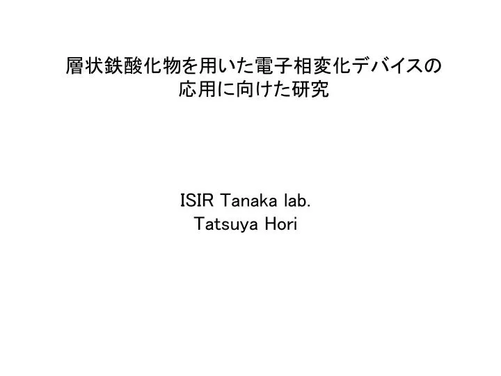
層状鉄酸化物を 用いた電子相変化デバイス の 応用に向けた研究. ISIR Tanaka lab. Tatsuya Hori. Differences between semiconductor device and Electronic phase transition device (EPT device). ( 電子相変化デバイス ). ・ Semiconductor device Current control is main feature. ・ EPT device

E N D
層状鉄酸化物を用いた電子相変化デバイスの 応用に向けた研究 ISIR Tanaka lab. Tatsuya Hori
Differences between semiconductor device and Electronic phase transition device (EPT device). (電子相変化デバイス) ・Semiconductor device Current control is main feature. ・EPT device Transition induce drastic changing of physical property. Unprecedented almost all new device. (Not only current control) ・Scaling merit Semiconductor EPT devices
What are EPT devices? Stimulation (T, H, E, N) Water H2O: Ice Metal Electrons: Insulator Applying the transition of stable electronic phase for electronics
Necessity for invention of EPT device Conceivable applications ・Optical switch ・Photochromic devices ・Magnetic modulators ・ESD protection devices ・etc… Considerable expectations… But only few device works in RT has invented
Candidate material for EPT device ReFe2O4 Fe/Odouble layer Fe3+:Fe2+=1:1 +or b c ? a Re/O + Interaction (Re = Dy, Ho, Er, Tm, Yb, Lu, Y) We can get the charge-ordering in room temperature. (= the state electrons are frozen)
Electronic field induced resistive switching in RT Electronic phase transition Resistive switching L. J. Zenget al., EPL84, 57011 (2008).
Motivations ・Fabricating the ReFe2O4 thin films, then observing the resistive switching phenomenon. ・For the electronics applying, investigate the switching phenomenon
What is PLD method? Laser Feature ・Suitable for high-melting-point materials. ・Easy to control thickness. ・In situ RHEED observation. ・etc… Heater Substrate Plasma plume Recipe Laser medium: ArF(l = 193nm) Tsub = 950˚C, pO2= 1×10⁻⁴ Pa Post-annealing: 800˚C, in vacuum (b.p. ~ 1×10⁻⁵ Pa) Gases Target
I could fabricate LuFe2O4 and YbFe2O4 thin films. Out-of-plane 2q/q scan 1/2Re2O3+2Fe+5/2O2ReFe2O4 * T = 1470 K * * * * * * * Achievable in our chamber * * (003) (006) (009) Ho Er Yb Lu Y Tm I succeeded in fabrication of LuFe2O4 and YbFe2O4 thin film. The orientation is ReFe2O4[001]//YSZ[111]
Revelation of charge-ordering LuFe2O4 YbFe2O4 Electron transport properties are same as that of bulks’. Existence of charge-ordering confirmed. EA = 0.21 0.26 (eV)
Interrelation between charge-ordering and switching YbFe2O4 LuFe2O4 310K 300K 3D 3D 2D 2D Resistive switching phenomenon is observed under 3D charge-ordering region
Conclusion ・I successfully fabricated ReFe2O4 thin films and observed resistive switching phenomenon in two systems. ・I got the data which imply switching phenomenon is observable under 3D charge-ordering region. From the above, I revealed this kind of switching phenomenon is common property of these charge-ordering systems. Fe/Odouble layer in ReFe2O4