Download
1 / 33
340 likes | 648 Views
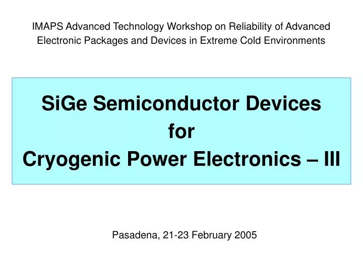
SiGe Semiconductor Devices for Cryogenic Power Electronics – III. IMAPS Advanced Technology Workshop on Reliability of Advanced Electronic Packages and Devices in Extreme Cold Environments. Pasadena, 21-23 February 2005. Outline. The Team and Coordination Goals & Applications

E N D
SiGe Semiconductor Devices for Cryogenic Power Electronics – III IMAPS Advanced Technology Workshop on Reliability of Advanced Electronic Packages and Devices in Extreme Cold Environments Pasadena, 21-23 February 2005
Outline • The Team and Coordination • Goals & Applications • Technical Objectives & Approach • SiGe Cryo Power HBTs • SiGe Cryo Power Converters • Summary & Plans
The Team R. R. Ward, W. J. Dawson, L. Zhu, R. K. Kirschman GPD Optoelectronics Corp., Salem, New Hampshire G. Niu, R. M. Nelms Auburn University, Dept. of Electrical and Computer Engineering, Auburn, Alabama O. Mueller, M. J. Hennessy, E. K. Mueller MTECH Labs./LTE, Ballston Lake, New York R. L. Patterson, J. E. Dickman NASA Glenn Research Center, Cleveland, Ohio A. Hammoud QSS Group Inc., Cleveland, Ohio
Coordination NASA SBIR Phase I and II DARPA STTR Phase I
Outline • The Team and Coordination • Goals & Applications • Technical Objectives & Approach • SiGe Cryo Power HBTs • SiGe Cryo Power Converters • Summary & Plans
Overall Goal • Semiconductor devices (diodes and transistors) • For power management and distribution (PMAD) • Electrical power storage and transmission • Power conversion for motors/generators • For superconducting or cryogenic systems • Temperatures down to ~20 K
NASA Interest • Cryogenic systems for spacecraft/aerospace • Cold Solar System sites • Fly-by, orbiting, landers, rovers, penetrators, ... • Propulsion systems • Power generation/storage/distribution systems
Specific NASA Technical Goals • Demonstrate SiGe devices at cryogenic temperatures, down to ~20 K • Device types: SiGe HBTs, MOSFETs, IGBTs • Demonstrate SiGe superiority over Si devices for cryogenic power circuits
Coordination Separate STTR Program from DARPA Phase I, June - December 2004 with Auburn University
NASA in bold, DARPA Phase II in gray Coordination – Goals
Outline • The Team and Coordination • Goals & Applications • Technical Approach • SiGe Cryo Power HBTs • SiGe Cryo Power Converters • Summary & Plans
Why SiGe? • Incorporate desirable characteristics of Si and Ge • Can optimize devices for cryogenic applications by selective use of Ge, Si and SiGe • SiGe provides additional flexibility through band-gap engineering (% of Ge) • Devices can operate at all cryogenic temperatures (as low as ~ 1 K if required) • All device types work at cryogenic temperatures • Diodes • Field-effect transistors • Bipolar transistors • Compatible with standard semiconductor processing
SiGe Bandgap 90 K G. Theodorou et al., “Structural, electronic, and optical properties of strained SiGe alloys,” Phys Rev B, vo.l 50, pp. 18355-18359, 15 Dec. 1994.
Outline • The Team and Coordination • Goals & Applications • Technical Objectives & Approach • SiGe Cryo Power HBTs • SiGe Cryo Power Converters • Summary & Plans
Emitter contact Base contact ~0.5 μm n+ Si ~0.4 μm p SiGe ~20 μm n– Si ~150 μm n+ Si Collector contact Cryo Power HBT Design Example
A Cryo Power HBT Die ~4 mm
Cryo Power HBT Characteristics LN RT 2 A 1 A 20 V 20 V IB = 5 mA Gain ~ 75 IB = 0.5 mA Gain ~ 500
Outline • The Team and Coordination • Goals & Applications • Technical Objectives & Approach • SiGe Cryo Power HBTs • SiGe Cryo Power Converters • Summary and Plans
+ Power supply – SiGe Boost Converter Circuit 24 V in 48 V out Inductor SiGe diode + Input capacitor Output capacitor Load SiGe HBT – Drive circuit ~10 – 300 K Switching pulse
Cryostat for Measuring 100 W Circuits(variable temperature 300 to ~20 K) ~ 4” Superinsulation Cooling channel (inside Cu block) ~ 8” Converter circuitry Cu thermal mass/mounting block Electrical feedthru Stainless steel tubes GHe vent LHe vendor’s dewar LHe
Outline • The Team and Coordination • Goals & Applications • Technical Objectives & Approach • SiGe Cryo Power HBTs • SiGe Cryo Power Converters • Summary & Plans
Summary • Cryogenic power conversion is of interest for a range of applications within NASA and elsewhere. • For cryogenic power conversion, SiGe devices are potentially superior to devices based on Si or Ge. • We have begun development of SiGe semiconductor devices (HBTs and MOSFETs) for cryogenic power applications. • We have designed, fabricated, and used SiGe HBTs in power converters operating at cryogenic temperatures and converting >100 W.
Plans • Improve SiGe HBT characteristics (especially at cryo temps) • By simulation • On voltage • Off breakdown voltage • Switching speed • Compare power converter performance at cryogenic temperatures, comparing SiGe HBTs to Si BJTs • Design, fabricate and use SiGe MOSFETs in cryogenic power circuits • If practical, fabricate SiGe IGBTs