Download
1 / 12
120 likes | 123 Views
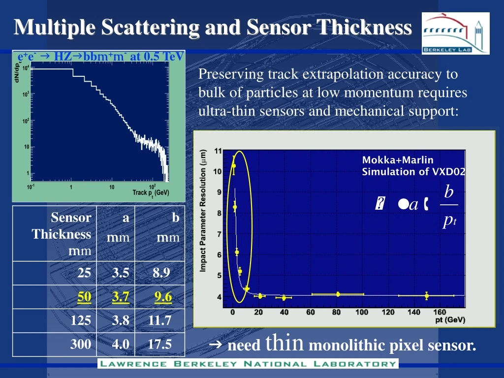
e + e - g HZ g bb m + m - at 0.5 TeV. Multiple Scattering and Sensor Thickness. Preserving track extrapolation accuracy to bulk of particles at low momentum requires ultra-thin sensors and mechanical support:. Mokka+Marlin Simulation of VXD02. g need thin monolithic pixel sensor.

E N D
e+e-g HZgbbm+m- at 0.5 TeV Multiple Scattering and Sensor Thickness Preserving track extrapolation accuracy to bulk of particles at low momentum requires ultra-thin sensors and mechanical support: Mokka+Marlin Simulation of VXD02 g need thin monolithic pixel sensor.
CMOS Sensor Back-thinning SiO + Metal Thin sensitive epi-layer makes CMOS Pixel sensors in principle ideally suited for back-thinning w/o significant degradation of performance expected (especially S/N), but questions arise from earlier results; Epi Si Bulk Si SEM Image of CMOS Pixel Chip Back-thinning of diced CMOS chips by partner Bay Area company: Aptek. Aptek uses grinding and proprietary hot wax formula for mounting die on grinding plate: Backthinning yield ~ 90 %, chip thickness measured at LBNL after processing: “50 mm” = mm , “40 mm” = mm; three chips fully characterised: Chip mounted on PCB with reversible glue and characterized Chip removed from PCB Back-thinning Chip re-mounted and re-characterized
40 mmBack-thinned Sensor Tests Study change in charge collection and signal-to-noise before and after back-thinning: Mimosa 5 sensors (IPHC Strasbourg), 1 M pixels 17 mm pitch, 1.8x1.8 cm2 surface 55Fe Determine chip gain and S/N for 5.9 keV X rays Collimated Laser Compare charge collection in Si at different depths 1.5 GeV e- beam Determine S/N and cluster size for m.i.p. S/N CMOS sensors back-thinning feasible NIM A579 (2007) 675
Extrapolation from experience at SLD VXD3 to STAR HFT Definition of overall material budget rescaled from VXD3 Su Dong/SiD
0.282% X0 STAR HFT Ladder Program of engineering design, construction and characterization of full ladder equipped with back-thinned CMOS pixel sensors based on experience from STAR HFT project and in collaboration with them; • STAR Low mass carrier: 50mm CFC+3.2mm RVC+50mm CFC (=0.11%X0);
STAR HFT Cable • ~ 100 traces (2 LVDS pairs / sensor, clk, power, gnd, cntl ) • 4 layer design, 25 µm kapton, 20 µm Al conductor • Impedance controlled signal / clock pairs with power and ground geometrically arranged as shielding. L Greiner, Snowmass 2005
T(0C) IR Camera Image Air Cooling Test Thin Chips Heating cable (80mW/cm2) STAR HFT Ladder Testing Mechanical and thermal characterization of STAR prototype, study of heat removal using low-speed airflow; r.m.s displacement on unsupported end of ladder mounted at one end, w/ quasi-laminar airflow at 20o angle STAR Prototype Capacitive Probe Measurement
STAR HFT Ladder Testing STAR study of accuracy of chip positioning on carrier: 50 mm back-thinned MIMOSA5 are positioned using a vacuum chuck with alignment bump edge and individual vacuum chuck valves; Chip Corner Locations Profile of Chip Elevation on Carrier Measurements using Optical Survey Machine with ~ 1 mm accuracy. Accurate to ~ 20 mm Flat to ~ 30 mm
VTX Ladder Design & Testing • Performed surveys of 40 mm and 50 mm thin chips and FEA analysis • of stress on flattened chip, results suggest sandwich ladder design; FEA stress analysis of flattened 50 mm chip Measured Surface Map of 50 mm thin chip 2 mm
VTX Ladder Design & Testing • Performed surveys of 40 mm and 50 mm thin chips and FEA analysis • of stress on flattened chip, results suggest sandwich ladder design;
VTX Ladder Design & Testing • FEA of prototype sandwich structure: • (core-cooled Si/CF/RVC sandwich, Si/Al/RVC sandwich); • Core-cooled ladder concept is promising, optimisation in progress to • move to prototyping in 2008; Vertex Tracker Design with core-cooled ladders Concept for Symmetric Ladder Sandwich Support with Air Cooling through Core Low density (0.2-0.6 g/cc) high thermal conductivity (40-180 W/m K) foam